
ST’ MEMS Studio is a new all-in-one tool for MEMS sensor evaluation and development, connected closely with the STM32 microcontroller ecosystem and available for Windows, MacOS, and Linux operating systems.
By unifying the sensor-development workflow, from evaluation to configuration and programming, MEMS Studio accelerates development and simplifies bringing rich contextual awareness to users’ projects. Enhanced features help easily acquire and clearly visualise sensor data to explore the operating modes and optimise performance and accuracy. There are also tools for pre-built library testing, as well as convenient drag-and-drop algorithm creation for intuitive, no-code development of STM32 MCU firmware.
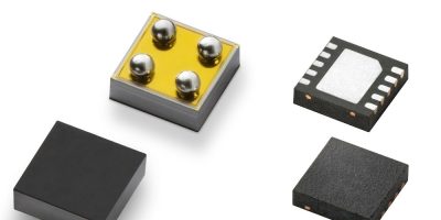
MEMS Studio supports the wide portfolio of ST MEMS sensors, including motion sensors, environmental sensors, and infrared sensors. It provides tools to explore and use all the sensors’ features including the finite state machine (FSM) and embedded edge AI in inertial modules for power-efficient inferencing directly in the sensor. These include creating and managing decision trees in sensors equipped with ST’s machine-learning core (MLC), monitoring interrupts status, and testing advanced features like FIFO, pedometer, and freefall detection embedded in the sensor.
MEMS Studio also offers a new experience for analysing sensor data in runtime and offline, where users can visualise, label, and edit the data for the best algorithm implementation. Spectrogram analysis and fast Fourier transform (FFT) are also available and help understand the sensor signal for the best detection of the sensing application target.
Users can choose from a wide variety of compatible development boards, including STM32 Nucleo expansion boards, sensor adapters, and ST’s multi-sensor evaluation kits. These comprise the SensorTile.box PRO, STWIN.box, and STEVAL-MKI109V3 professional MEMS adapter motherboard with adjustable power settings and a STM32F401VE MCU on-board.
As creative use of MEMS sensors continues to drive innovation in cutting-edge applications, MEMS Studio empowers designers to add new and more advanced functions in next-generation high-tech products. Its release promotes the development of smart appliances, medical wearables, and technology for digital healthcare, smart buildings and factories, robotics, asset tracking, and smart driving.
Consolidating and extending the features of established sensor-development tools including AlgoBuilder, Unico-GUI, and Unicleo-GUI, MEMS Studio is available now to download, free of charge, from https://www.st.com/mems-studio.