
Developed to ensure seamless connectivity even when no terrestrial cellular network is available, the u-blox SARA-S520M10L is the company’s cellular and satellite IoT module with accurate, low power positioning and “ubiquitous connectivity” said u-blox.
The module’s communication and tracking capability makes it suitable for asset tracking, fleet management, maritime transportation, mining, utilities and smart agriculture applications. It also serves market segments such as anti-theft systems, industrial monitoring and control, and applications that require communication in safety-critical scenarios, advised u-blox.
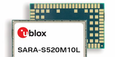
At approximately 400mm2, the u-blox SARA-S520M10L is claimed to be the smallest multi-mode cellular and satellite IoT module on the market. It provides LTE-M/NB-IoT, L-band satellite connectivity, and embedded navigation capability for connectivity through terrestrial cellular networks and geostationary (GEO) satellites. It can provide location fixes using up to four satellite constellations and is pin-compatible with other u-blox cellular-only modules in the SARA form factor.
This is the first u-blox module designed with the 2nd generation of the u-blox UBX-R5 chip, the UBX-R52/S52. The S52 variant was developed to support satellite IoT communication alongside LTE-M/NB-IoT cellular standards.
“Comparable solutions on the market require two distinct subsystems, one for cellular and another for satellite connectivity,” said Alessandro Bonetti, senior product manager, product centre cellular at u-blox. Building the module around a single, highly integrated, multi-mode modem SoC reduces size and complexity, Bonetti added. He said the versatile SoC, combined with the company’s GNSS capability serves mobile and stationary IoT applications in “challenging environments such as isolated places, mountains, or in the middle of the ocean”.
The first samples will be available by Q1 2024.
u-blox specialises in positioning and wireless communication in automotive, industrial and consumer markets. The company’s services, and products let people, vehicles, and machines determine their precise position and communicate wirelessly over cellular and short range networks. It offers a broad portfolio of chips, modules, and secure data services and connectivity to develop solutions for the IoT quickly and cost-effectively. With headquarters in Thalwil, Switzerland, the company has offices in Europe, Asia, and the USA.