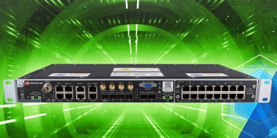
Ceva extends its Connect IP Portfolio with Wi-Fi 7 platform for high-end consumer and industrial IoT

Ceva has announced the general release of its next generation RivieraWaves Wi-Fi 7 IP platform, further expanding its widely-licensed portfolio of connectivity IP, targeting high-end consumer and industrial applications including gateways, TVs, set-top-boxes, streaming media devices, AR/VR headsets, personal computing and smartphones. The RivieraWaves Wi-Fi 7 IP leverages all the latest advanced features of the IEEE 802.11be standard to deliver a premium high performance, cost- and power-optimised Wi-Fi solution for integration into the next wave of Wi-Fi Access Point (AP) and Station (STA) products.

According to global technology intelligence firm ABI Research, annual Wi-Fi enabled chipset shipments will exceed 5.1 billion by 2028, with more than 1.7 billion of these chipsets supporting the Wi-Fi 7 standard. As Wi-Fi enabled device shipments continue to grow, increasing numbers of semiconductor companies and OEMs are choosing to integrate Wi-Fi connectivity into their chip designs, and need access to high quality Wi-Fi IP to reduce the development costs and risks. Spanning Wi-Fi 4/5/6 over the past decade, Ceva has already established a considerable leadership position in Wi-Fi IP licensing, with more than 40 licensees for its RivieraWaves Wi-Fi 6 IP family, serving a wide range of end markets and applications, from end points to access points, across the IoT sphere. Expanding on this leadership position, Ceva’s RivieraWaves Wi-Fi 7 IP provides a unique, comprehensive 802.11be MAC and PHY solution for integration into the next generation of Wi-Fi SoC products.

Andrew Zignani, Senior Research Director, ABI Research, commented: “Ceva’s wireless connectivity IPs play an integral role in the proliferation of connectivity standards in the broad IoT markets, as is evident from their customer’s success in shipping more than 1 billion connectivity chips annually. With the introduction of their RivieraWaves Wi-Fi 7 IP platforms, semiconductor companies and OEMs have a trusted partner to develop differentiated, high-performance Wi-Fi 7 chipsets for their connectivity roadmaps, with lower risk and a lower cost of ownership.”

Tal Shalev, Vice President and General Manager of the Wireless IoT BU at Ceva, stated: “The relentless expansion of Wi-Fi usage has pushed the Wi-Fi 7 standard to offer enhanced data throughput, improved latency and support more spectrum in the face of mounting network congestion. Achieving this requires highly complex, cutting-edge functionalities like 4K QAM modulation, Multi Link Operation and Multi Resource Unit to optimize link efficiency across the available bands. Our RivieraWaves Wi-Fi 7 IP platform incorporates all the features of this latest-generation, wireless standard, dramatically simplifying development and time-to-market for companies looking to add Wi-Fi 7 connectivity to their products.”

Wi-Fi 7’s 4K QAM modulation scheme is a substantial increase on the previous 1K QAM of Wi-Fi 6, while Multi Link Operation (MLO) introduces dynamic channel aggregation, seamlessly combining heterogenous channels from the same or different bands to navigate interference and boost throughput. Similarly, Multi Resource Units (MRU) enables the creation of larger channel bandwidths by intelligently stitching together punctured or disjointed Resource Units within the same band. The outcome is not only a remarkable up to 5 times increase in raw speeds but also significantly reduced latency, thanks to diminished contentions and retries.

visit https://www.ceva-ip.com/product/rivierawaves-wi-fi-platforms/.


> Read More

Mouser signs global distribution agreement with Ambiq to deliver ultra-low power AI microcontrollers

Mouser has announced a new global distribution agreement with Ambiq, a leading supplier of low-powered, AI-enabled microcontrollers for wearables, hearables, IoT, edge devices and mobile edge computing applications.

“We are pleased to announce our partnership with Ambiq, which furthers our commitment to providing the latest products and technologies to our customers worldwide,” said Kristin Schuetter, Vice President of Supplier Management at Mouser Electronics. “We look forward to providing engineers and buyers worldwide with their innovative embedded solutions, backed by Mouser’s best-in-class logistics and unsurpassed customer service.”

“Mouser is well-known for its worldwide distribution and support system,” said Mike Kenyon, Vice President of Sales and Business Development at Ambiq. “We are excited to enter into this relationship. With distribution through Mouser, we can draw on their expertise in delivering leading-edge technologies and expand our global customer base.”

Among the Ambiq products now available from Mouser are the Ambiq Apollo4 Blue Lite system-on-chip (SoC) and the Ambiq Apollo4 Blue Lite evaluation board. The Apollo4 Blue Lite SoC features a 32-bit Arm® Cortex®-M4 core with a Floating-Point Unit, along with a Bluetooth® Low Energy 5.1 radio with robust RF connectivity. This SoC is ideal for use in battery-powered endpoint devices, including smartwatches, fitness bands, animal trackers, voice-activated remotes and digital health products. The Ambiq Apollo4 Blue Lite evaluation board offers a complete demonstration and development platform for the Apollo4 Blue Lite device.

Mouser also offers the Apollo3 Blue Plus evaluation board and the Apollo3 Blue Plus SoC. The Apollo3 Blue Plus device is based on Ambiq’s Voice-on-SPOT (VoS) platform, making it the perfect microprocessor for enabling always-on voice assistant integration and command. The Apollo3 Blue Plus evaluation board enables quick and easy prototyping of the SoC. The Apollo3 Blue Plus Voice-on-SPOT kit, also available from Mouser, facilitates demos, evaluation, and the development of ultra-low power audio and voice capabilities on the Apollo3 Blue Plus SoC. The kit provides always-on voice capability with options for one or two microphones, signal processing, wake word/command detection, codec, and Bluetooth Low Energy communication.

The Artasie AM1805 evaluation board offers an easy method to measure and evaluate Ambiq’s AM18x5 real-time clocks. The evaluation board includes on-chip oscillators to provide minimum power consumption, full RTC functions including battery backup and programmable counters and alarms for timer and watchdog functions, and a PC serial interface for communication with a host controller.

To learn more about Ambiq products available from Mouser, visit https://www.mouser.com/manufacturer/ambiq/.

> Read More

R&S verifies NXP’s next generation automotive radar sensor reference design for extremely short object distances

The radar target simulator R&S RTS has been used to verify the performance of NXP® Semiconductors’ next-generation radar sensor reference design. This collaboration enables the automotive industry to take another step forward in the development of automotive radar, the principal technology that enables advanced driver assistance systems (ADAS) and autonomous driving features.

Engineers from both companies conducted a comprehensive series of tests to verify the new sensor reference design which is based on a NXP’s 28 nm RFCMOS radar one-chip SoC (SAF85xx). The R&S RTS radar test system combines the R&S AREG800 automotive radar echo generator with the R&S QAT100 antenna mmW frontend, offering unique short-distance object simulation capabilities as well as superior RF performance and advanced signal processing with many advanced functions. This enables realistic tests of next generation automotive radar applications and brings automotive industry’s vision of fully autonomous driving one step closer.

NXP’s next generation automotive radar sensor reference design is enabled by the industry’s first 28 nm RFCMOS radar one-chip SoC family leveraging the R&S RTS radar test system. The radar sensor reference design can be used for short, medium and long-range radar applications to serve challenging NCAP (NCAP: New Car Assessment Program) safety requirements as well as comfort functions like highway pilot or urban pilot for the fast-growing segment of L2+ and L3 vehicles.

The R&S RTS is the only test system suitable for complete characterisation of radar sensors and radar echo generation with object distances down to the airgap value of the radar under test. It combines the R&S AREG800A automotive radar echo generator as a backend and the R&S QAT100 antenna array or the R&S AREG8-81S as a frontend. The technically superior test solution is suitable for the whole automotive radar lifecycle including development lab, hardware-in-the-loop (HIL), vehicle-in-the-loop (VIL), validation and production application requirements. The solution is also fully scalable and can emulate the most complex traffic scenarios for advanced driver assistance systems.

Adi Baumann, Senior Director ADAS R&D, at NXP Semiconductors says: “We have been collaborating closely and successfully with Rohde & Schwarz for many years on the verification of our automotive radar sensor reference designs. Rohde & Schwarz’ cutting-edge automotive radar test systems allows us high-quality and highly efficient validation of our automotive radar products and proves outstanding performance of our radar one-chip. The level of experience, quality and support that Rohde & Schwarz provides to NXP is making a difference.”

Gerald Tietscher, Vice President Signal Generators, Power Supplies and Meters from Rohde & Schwarz says: “We are grateful for the collaboration with NXP to accelerate the deployment of advanced automotive radar sensors based on 28 nm automotive radar chips. They serve ever more challenging NCAP safety requirements and will help enable new safety applications. Our experience in automotive radar testing allows us to provide a best-in-class test solution for this radar sensor design based on the industry’s first 28 nm RFCMOS one-chip radar SoC.”

NXP will present the latest developments for radar including the automotive radar sensor reference design at CES 2024 trade show in Las Vegas from January 9 to 12, 2024, at booth CP18.

https://www.rohde-schwarz.com/

> Read More

New, robust approach to overvoltage protection for sensitive electronic signal inputs

High demands on the robustness of electronic systems, especially in industrial environments, continually present developers with great challenges. Overvoltage protection is one key design consideration and challenge, as additional components are usually required to protect systems from overvoltage events – yet they frequently impact and, in the worst case, can even falsify signals. Beyond that, these components incur additional costs and contribute to spatial constraints. Hence, when designing the protection circuit, traditional solutions often require a compromise between system accuracy and the protection level.

Typically, a common and simple design method uses external protection diodes, usually transient voltage suppressor (TVS) diodes, clamped between the signal line and supply or ground. TVS diodes are advantageous as they can react instantaneously to temporary voltage spikes. This type of external overvoltage protection is shown on the left side of Figure 1.

Figure 1. Traditional overvoltage protection design with additional discrete components.
If a positive transient voltage pulse occurs, it is clamped with a current through diode D1 to VDD. The voltage is thereby limited to VDD plus the diode forward voltage. If the pulse is negative and less than VSS, the same applies with the exception that it is clamped to VSS via D2. However, if the leakage current caused by the overvoltage is not limited, it may damage the diodes. For this reason, there is also a current-limiting resistor in the path. For very harsh environmental conditions, an input-side bidirectional TVS diode is often used for enhanced protection.
The disadvantages resulting from this type of protection circuit appear – for example, in the form of increased edge rise and fall times and capacitive effects. Moreover, it doesn’t provide any protection when the circuit is in the de-energised state.
The actual components, such as analogue-to-digital converters (ADCs), operational amplifiers, etc., usually have integrated protection. This can consist of a switch architecture, as shown on the right side of Figure 1. Figure 1 also shows that input-side and output-side protection diodes are present on both supply rails. The downside to this setup is that, when floating signals appear in a de-energized state (the IC is not powered up), the switch may act as if it is active (even if it is set to OFF) as current will flow through the diodes and the power supply rails. This allows current to pass through, resulting in the signal line losing its protection.

Fault-Protected Switch Architecture
One solution to the challenges mentioned above is a fault-protected switch architecture supplemented by a bidirectional ESD cell, as can be seen in Figure 2. Instead of the input-side TVS diodes, now the ESD cell clamps voltage transients by constantly comparing the input voltage with VDD or VSS. In the case of permanent overvoltage, the downstream switch opens automatically. The input voltage is no longer limited by the protection diodes clamped to the supply rails. The limiting factor is now the maximum voltage rating of the switch. Higher system robustness and reliability are additional advantages. There is also virtually no effect on the actual signals and their accuracy. Moreover, the additional current-limiting resistor is not needed because the leakage currents are very low when the switch is open.

Figure 2. Overvoltage protection with integrated bidirectional ESD cell.

This type of input structure is characteristic of the quad SPST (single-pole, single-throw) switch ADG5412F from Analog Devices Inc. (ADI). This switch permits a permanent overvoltage of up to ±55V, regardless of any existing voltage supply. The ESD cell integrated on each of the four channels clamps voltage transients of up to 5.5kV. In an overvoltage condition, only the affected channel is opened and the other channels continue operating normally.

Conclusion
Thanks to this type of overvoltage protection switches, electrical circuits can be greatly simplified. The advantages over the conventional discrete solution are multitudinous, both in terms of guaranteeing optimal switching performance and robustness in a precise signal chain and in terms of spatial optimisation. Hence, the overvoltage protection offered by the ADG5412F is especially suitable for high precision measurement applications in harsh environments.

About the Author
Thomas Brand began his career at Analog Devices in Munich in 2015 as part of his master’s thesis. After graduating, he was part of a trainee program at Analog Devices. In 2017, he became a field applications engineer. Thomas supports large industrial customers in Central Europe and also specialises in the field of Industrial Ethernet. He studied electrical engineering at the University of Cooperative Education in Mosbach before completing his postgraduate studies in international sales with a master’s degree at the University of Applied Sciences in Constance. He can be reached at thomas.brand@analog.com.


> Read More

About Smart Cities

This news story is brought to you by smartcitieselectronics.com, the specialist site dedicated to delivering information about what’s new in the Smart City Electronics industry, with daily news updates, new products and industry news. To stay up-to-date, register to receive our weekly newsletters and keep yourself informed on the latest technology news and new products from around the globe. Simply click this link to register here: Smart Cities Registration