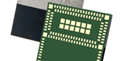
Infineon introduces the OPTIGA Trust M MTR, making it easy to add Matter and security to smart home devices

In a world of increasing connectivity and the growing popularity of the Internet of Things, it is important to simplify interoperability across connected devices and to enhance their security and reliability. The Matter standard was created precisely for this purpose. In order to facilitate integration of the Matter standard and security features into smart home and smart building devices, Infineon has introduced the OPTIGA Trust M MTR. The Matter-certified secure element is the latest configuration of Infineon’s OPTIGA Trust M, combined with a Matter provisioning service.

According to ABI Research forecasts, the number of smart home devices will double by 2030, reaching about 1.7 billion worldwide. All these devices have to be able to connect securely and reliably with each other and with different smart home ecosystems. That’s where the Matter standard comes into play, facilitating smooth interoperability across connected devices even from different companies. The Matter protocol defines a set of principles that support uniform security and privacy measures for the smart home, since smart homes rely on smart devices to increase not only comfort but also efficiency and security.

The tamper-resistant security controller can be easily integrated into a system to perform security-related functions and provide a high level of protection for sensitive data and cryptographic operations. As a discrete Secure Element, OPTIGA Trust M MTR can be integrated into any MCU-based design to enhance security and handle multiple product protocols simultaneously. This gives original equipment manufacturers greater flexibility and allows faster time to market.

According to the Matter protocol, every smart home device must have a Device Attestation Certificate (DAC), containing the Product ID (PID) and the Vendor ID (VID), to verify the authenticity and trustworthiness of each device commissioned in the Matter ecosystem. With OPTIGA Trust M MTR, the PID no longer needs to be defined in advance when the reel is ordered or manufactured. Instead, each device receives a personalised DAC injection at a later point right up until the start of device production. This gives device manufacturers more flexibility in creating multiple product variants of smart home devices.

OPTIGA Trust M MTR secure elements are pre-provisioned at a Common Criteria-certified Infineon facility. The batch of Secure Elements on a reel is shipped with an associated barcode. The customer claims ownership of these chips on the IoT portal of Infineon partner Kudelski IoT by scanning the barcode. Kudelski IoT is a trusted and established Product Attestation Authority (PAA) approved by the Connectivity Standards Alliance (CSA). Kudelski IoT will enable the download of production DACs corresponding to the vendor and the product. Finally, the personalised DAC is transferred to the OPTIGA Trust M MTR at the factory level (see graphic).

Samples of OPTIGA Trust M MTR are available now together with the OPTIGA Trust M MTR Shield for easy evaluation and design-in. Availability for the broad market will begin in March 2024. In addition, developers can rely on design-in application notes and extensive host-side integration support without having to sign a non-disclosure agreement (NDA). Moreover, Infineon offers training measures for the security products. More information is available at www.infineon.com/OPTIGA-Trust-M-MTR.

https://www.infineon.com

> Read More

Renesas announces ultra-fast MRAM test chip for IoT and AI devices

Renesas has announced that it has developed circuit technologies for an embedded spin-transfer torque magnetoresistive random-access memory (STT-MRAM, hereinafter MRAM) test chip with fast read and write operations. Fabricated using a 22-nm process, the microcontroller unit (MCU) test chip includes a 10.8-megabit (Mbit) embedded MRAM memory cell array. It achieves a random read access frequency of over 200 MHz and a write throughput of 10.4-megabytes-per-second (MB/s).

As IoT and AI technologies continue to advance, MCUs used in endpoint devices are expected to deliver higher performance than ever. The CPU clock frequencies of high performance MCUs are in the hundreds of MHz, so to achieve greater performance, read speeds of embedded non-volatile memory need to be increased to minimise the gap between them and CPU clock frequencies. MRAM has a smaller read margin than the flash memory used in conventional MCUs, making high speed read operation more difficult. On the other hand, for write performance, MRAM is faster than flash memory because it requires no erase operation before performing write operations. However, shortening write times is desirable not only for everyday use, but also for cost reduction of writing test patterns in test processes and writing control codes by end product manufacturers.

MRAM reading is generally performed by a differential amplifier (sense amplifier) to determine which of the memory cell current or the reference current is larger. However, because the difference in memory cell currents between the 0 and 1 states (the read window) is smaller for MRAM than for flash memory, the reference current must be precisely positioned in the centre of the read window for faster reading. The newly developed technology introduces two mechanisms. The first mechanism aligns the reference current in the centre of the window according to the actual current distribution of the memory cells for each chip measured during the test process. The other mechanism reduces the offset of the sense amplifier. With these adjustments, faster read speed is achieved.

Furthermore, in conventional configurations, there is large parasitic capacitance in the circuits used to control the voltage of the bitline so it does not rise too high during read operations. This slows the reading process, so a Cascode connection scheme is introduced in this circuit to reduce parasitic capacitance and speed up reading.

Thanks to these advances, Renesas can achieve the world’s fastest random read access time of 4.2 ns. Even taking into consideration the setup time of the interface circuit that receives the MRAM output data, we can realize the random read operation at frequencies in excess of 200 MHz.

For the write operation, the high-speed write technologies for embedded STT-MRAM announced in December 2021 improved write throughput by first applying write voltage simultaneously to all bits in a write unit using a relatively low write voltage generated from the external voltage (IO power) of the MCU chip through a step-down circuit, and then used a higher write voltage only for the remaining few bits that could not be written. This time, Renesas takes into account that because the power supply conditions used in test processes and by end product manufacturers are stable, the lower voltage limit of the external voltage can be relaxed. Thus, by setting the higher step-down voltage from the external voltage to be applied to all bits in the first phase, write throughput can be improved 1.8-fold.

Combining the above new technologies, a prototype MCU test chip with a 10.8Mbit MRAM memory cell array was fabricated using a 22 nm embedded MRAM process. Evaluation of the prototype chip confirmed that it achieved a random read access frequency of over 200 MHz and a write throughput of 10.4 MB/s at a maximum junction temperature of 125°C.

The test chip also contains 0.3 Mbit of OTP (Note 2) that uses MRAM memory cell breakdown to prevent falsification of data. This memory can be used to store security information. Writing to OTP requires a higher voltage than writing to MRAM, making it more difficult to perform writing in the field, where power supply voltages are often less stable. However, by suppressing parasitic resistance within the memory cell array, this new technology also makes writing in the field possible.

https://www.renesas.com

> Read More

Infineon introduces lower cost Bluetooth long-range module for low power applications

Infineon has announced the CYW20822-P4TAI040, its latest Bluetooth module that pushes the low-power and range boundaries for wireless connectivity in IoT and consumer electronics. This module offers seamless integration, enhanced performance with Bluetooth low-energy long-range (LE-LR) support, and exceptional reliability for a wide range of applications. With the right combination of low power and high performance, Infineon’s CYW20822-P4TAI040 is designed to support the entire spectrum of Bluetooth LE-LR use cases including industrial IoT applications, smart home, asset tracking, beacons and sensors, and medical devices.

According to a recent report by ABI Research future use cases will demand additional improvements across almost all metrics. These include industrial IoT applications such as sensing, robotics, beacons, smart home, and asset tracking. In response, Infineon’s CYW20822-P4TAI040 Bluetooth module delivers unparalleled connectivity and performance, enabling customers to create innovative products in the IoT and consumer electronics space.

With extensive experience in delivering certified Bluetooth and Bluetooth LE modules, Infineon’s regulatory testing (FCC, ISED, MIC, CE) and certification process with the Bluetooth SIG is precise and rigorous. Its pre-certified modules are optimised for cost, size, power, and range.

“Infineon is thrilled to expand its Bluetooth portfolio with the introduction of the CYW20822-P4TAI040 Bluetooth module to help designers get to market faster,” said Anurag Chauhan, Director of Marketing for the Bluetooth product line at Infineon Technologies. “As a leader in the IoT area in delivering innovative new Bluetooth LE solutions, this new module is a testament to our customer commitment. This new module delivers low power, long range, and excellent RF performance to meet our customers evolving needs.”

Infineon’s CYW20822-P4TAI040 Bluetooth LE module is currently sampling. More information is available at https://www.infineon.com/CYW20822-P4TAI040

> Read More

Industry’s first Grandmaster to provide high-speed network interfaces up to 25 Gbps

The operators of critical infrastructure market segments such as 5G telecommunications, power utilities and transportation need to continuously upgrade their networks with technology capable of delivering higher processing speeds and highly accurate time sources that are not dependent on the Global Navigation Satellite System (GNSS) constellations like GPS, GALILEO and QZSS. To provide network operators a terrestrial alternative for distributing very accurate time, Microchip has announced the new TimeProvider 4500 grandmaster, a hardware timekeeping platform that provides high-speed network interfaces up to 25 Gbps and enables precise time accuracy of less than one nanosecond.

The TimeProvider 4500 grandmaster is capable of supporting very-high-capacity Precision Time Protocol (PTP) transactions. The innovative hardware platform enables higher IEEE-1588 scalability for thousands of clients. In network locations where range and capacity need to be balanced, namely in C-band 5G deployments, it is critical to be able to serve thousands of gNodeB from a single grandmaster. Depending on the specific sites, the grandmaster could serve very few or a large number of gNodeB base stations. This results in cost-effective and flexible deployments for operators regardless of scale.

The TimeProvider 4500 grandmaster offers the flexibility to connect to various generations of network elements, which helps to preserve operators’ infrastructure investments. The TimeProvider 4500 clock is the first 1588 grandmaster with 25 Gbps support. A customer can connect the TimeProvider 4500 clock to various network devices using a choice of 1 Gbps, 10 Gbps or 25 Gbps network links. High-speed bandwidth is essential as network element upgrades are migrating towards equipment that requires a minimum of 10 Gbps and, in some cases, up to 100 Gbps.

The extremely high time accuracy of the TimeProvider 4500 grandmaster is particularly important as operators are trying to deploy alternative solutions to GNSS.

A terrestrial option is often considered an attractive solution that can leverage existing optical network deployments to avoid the reliance on GNSS, thus providing a cost-effective way of transferring highly accurate time over long distances. The need for long-distance transfers translates into a requirement for ever- increasing accuracy needs at the source and regeneration of the time signal.

The TimeProvider 4500 grandmaster features new hardware assist enhancements, such as the latest generation of digital synthesiser and Microchip’s PolarFire SoC FPGA. These platform enhancements enable the system to move into the picosecond time accuracy realm.

“Microchip continues to develop new and innovative time and frequency solutions for critical infrastructure. We designed the TimeProvider 4500 clock to deliver tighter timing accuracy on existing optical network environments without the need for costly upgrades or dedicated dark fiber,” said Randy Brudzinski, vice president of Microchip’s frequency and time systems business unit. “This solution is also the first grandmaster with high-speed data processing up to 25 Gbps, enabling connectivity with the newest network elements in deployments.”

The advanced hardware platform of the TimeProvider 4500 clock supports all the features of the TimeProvider 4100 clock to ensure that operators deploying the new product can also benefit from their investments in the TimeProvider 4100 series. TP4500 adds specific capabilities above and beyond TP4100 due to its enhanced hardware platform.

The TimeProvider 4500 grandmaster is integrated with the TimePictra synchronisation management solution that enables operators to monitor and track real-time troubles and threats with visibility across their entire network. Other key functions of the TimePictra platform include comprehensive Fault, Configuration, Accounting (Inventory), Performance and Security (FCAPS) management functions; geographical topology and domain navigation; user preference dashboard customisation, intuitive web GUI for easy management and more.

https://www.microchip.com

> Read More

About Smart Cities

This news story is brought to you by smartcitieselectronics.com, the specialist site dedicated to delivering information about what’s new in the Smart City Electronics industry, with daily news updates, new products and industry news. To stay up-to-date, register to receive our weekly newsletters and keep yourself informed on the latest technology news and new products from around the globe. Simply click this link to register here: Smart Cities Registration