HD LCD video controller has MIPI-CSI2 input for parking assist

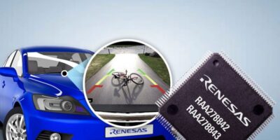
Claimed to be the first full HD 1080p LCD video controller to include a four-lane MIPI-CSI2 input, the RAA278842 LCD video controller’s four-lane (or dual two-lane) MIPI-CSI2 input supports up to 1Gbit per second per lane. This allows it to interface with the latest generation of automotive cameras, application processors and graphics processors, explains Renesas Electronics. The controller also supports a 150 MHz single-channel OpenLDI interface and a variety of video interfaces and LCD panel sizes with resolutions up to 1920 x 1080.

The RAA278842 can be used for automotive central infotainment displays (CIDs) and head units, instrument clusters, head-up displays (HUDs) and mirror replacement display applications for advanced driver assistance systems (ADAS).

“The RAA278842 LCD video controller helps automotive system manufacturers develop versatile and reliable display systems that provide superior HMI graphics for analogue and digital video content,” said Niall Lyne, senior director, automotive mixed-signal/power and video, Renesas Electronics. “Our strong heritage in video signal processing for backup cameras along with highly differentiated new technology is valued by automakers and Tier-1 suppliers worldwide,” he said.

The RAA278842 LCD video controller has 10-bit per colour processing built into the image enhancement engine to provide near-zero latency, high quality video. Integrated video diagnostics detect if the incoming video is frozen or corrupted and can provide a direct path for the rear camera video to be displayed on the LCD. This significantly improves rear camera display reliability, explains Renesas, claiming that it virtually eliminates the possibility of a software-related problem causing the rear camera video to be displayed incorrectly or not at all. The RAA278842 can display the camera image on an LCD in less than 500 milliseconds, addressing the fast boot requirement of many OEMs. The EEPROM/SPI flash fast boot allows register programming without requiring an external microcontroller

The RAA278842 with MIPI-CSI2 output and the RAA278843 with traditional BT.656 output, work with the system’s main processor to monitor the camera and the video data coming from the SoC or graphics processor unit (GPU). After vehicle ignition, while the instrument cluster boots up, the RAA27884x controller can display the carmaker’s logo or live camera video. The controller’s on-screen display feature can also simulate warning lamp checks in an instrument cluster application.

Both controllers enable compliance with FMVSS-111, requiring the blind spot area behind the vehicle is displayed in less than two seconds after the driver places the vehicle in reverse gear.

Proprietary input switching eliminates flicker when switching between sources, claims Renesas and the AEC-Q100 Grade-2 qualified devices are specified for operation from -40 to +105 degrees C

The RAA278842 and RAA278843 can be combined with Renesas’ R-Car SoC family, RH850 MCU family, and RL78 MCU family, as well as the ISL78302 dual LDO, ISL78322 dual 2A/1.7A synchronous buck regulator, and ISL78228 dual 800mA synchronous buck regulator to provide power rails for the RAA27884x and other ICs on the automotive infotainment system board.

Mass production quantities of the RAA278842 with MIPI-CSI2 output are available now in a 14 x 14mm, 128-lead LQFP package.

Mass production quantities of the RAA278843 with BT.656 output are available now in a 14mm x 14mm, 128-lead LQFP package.

http://www.renesas.com

> Read More

RS Components introduces compact IR temperature sensor for smart factories

Designed for space-sensitive factory maintenance, repair and operations (MRO) in smart manufacturing environments, the RS Pro infra red temperature sensor by RS Components is a low-cost non-contact voltage-output temperature sensor.

It has been designed to fit into tight spaces and show the measured temperature in- situ, so maintenance engineers do not have to return to the control room to check it.

The RS Pro infra red temperature sensor measures just 30mm deep and 31mm in diameter. It has a side-entry cable making it easy to mount in small spaces. The temperature is displayed on a built-in backlit OLED display, without the need for contact with the target surface. The sensor can be used where it is not possible to use contact probes, for example when the target is moving or inaccessible; it will fit between a wheel and the rim or hub of a disc brake.

The RS Pro infra red temperature sensor can measure surface temperatures from 0 to 1,000 degrees C to an accuracy of ±1.5 per cent of reading or ±1.5 degrees C, whichever is greater, and repeatability of ±0.5 per cent of reading or ±0.5 degrees C. Response time is just 250ms, allowing continuous monitoring by industrial process instrumentation via the DC voltage output.

The sensor provides simultaneous voltage and alarm outputs. The voltage output can be configured as 0 to 5V DC, 1.0 to 5V DC or 0 to 10V DC, with adjustable temperature range scaling, configured using built-in controls on the sensor. The open-collector alarm output offers adjustable temperature threshold and hysteresis.

The sensor is supplied set up to measure non-reflective surfaces such as paper, plastics, rubber, wood, tarmac, food, pharmaceuticals, organic materials and painted metal. To measure the temperature of reflective solid or liquid surfaces, the user can adjust emissivity settings between 0.20 and 1.00.

The RS PRO infra red temperature sensor is fitted with a 1m long cable, as standard. This can be extended using terminal blocks or connectors. An optional air purge collar helps keep the lens clean from smoke, fumes, dust, steam or other potential contaminants.

The device is IP65-rated.

https://uk.rs-online.com

> Read More

HBI+ PHY supports 2.5D interconnect for SoC partitioning

7nm high bandwidth interconnect (HBI+) PHY for die-to-die interconnects from eSilicon supports 2.5D applications such as silicon interposers and silicon bridges for system on chip (SoC) to chiplets and SoC partitioning.

The 7nm HBI+ physical interface (PHY) IP is available for license for customer designs. The hard IP block delivers a high-bandwidth, low-power and low-latency wide-parallel, clock-forwarded PHY interface for 2.5D applications including SoC to chiplets and SoC partitioning for complex sub-systems. Silicon interposer and silicon bridge technologies are supported, adds eSilicon.

The HBI+ PHY delivers a data rate of up to 4.0Gbits per second per pin. Flexible configurations include up to 80 receive and 80 transmit connections per channel and up to 24 channels per PHY, with one redundant lane per channel to improve production yields. The part also supports built-in self-test (BIST), internal loopback and external PHY-to-PHY link tests. It supports IEEE 1149.1 (JTAG) and 1149.6 (AC JTAG) boundary scan standards.

Hugh Durdan, vice president, strategy and products at eSilicon, said: “This new HBI+ PHY will help to enable a growing chiplet ecosystem that is supported by many new and innovative technologies.”

The earlier version of this PHY (HBI, 2.5 Gbits per second per pin) was used successfully on a customer ASIC at 14nm. eSilicon is currently in design with a major customer ASIC in 7nm using the HBI+ PHY.

eSilicon provides complex FinFET ASICs, market-specific IP platforms and advanced 2.5D packaging solutions. Its ASIC-proven, differentiating IP includes configurable 7nm 56G/112G SerDes plus networking-optimised 16, 14 or 7nm FinFET IP platforms featuring HBM2 PHY, TCAM, specialised memory compilers and I/O libraries. The company’s neuASIC platform provides AI-specific IP and a modular design methodology to create adaptable, efficient artificial intelligence (AI) ASICs. eSilicon serves the high-bandwidth networking, high-performance computing, AI and 5G infrastructure markets.

http://www.esilicon.com

> Read More

Clock generators, buffers and PCIe clocks and buffers are AEC-Q100-qualified

To meet the demanding clocking needs of in-vehicle systems, Silicon Labs believes it now offers the industry’s broadest portfolio of automotive grade timing solutions, as it introduces AEC-Q100-qualified timing devices, the Si5332 any-frequency programmable clock generators, Si5225x PCIe Gen1/2/3/4/5 clocks, Si5325x PCIe buffers and Si5335x fanout clock buffers.

These timing devices help automotive OEMs and Tier 1 suppliers simplify clock tree design, reduce system points of failure, increase system reliability and optimise the performance of high-speed serial data transfer. The timing devices target automotive camera sub-systems, radar and lidar sensors, advanced driver assistance systems (ADAS), autonomous driving control units, driver monitoring cameras, infotainment systems, Ethernet switches, and GPS and 5G connectivity.

Rather than using more quartz-based components to satisfy a growing list of timing requirements, developers now have the option to simplify their clock tree designs and increase system reliability using the company’s automotive-grade low-jitter, any-frequency clock generators and buffers.

Quartz crystal and oscillator timing devices can be prone to shock and vibration failure as well as start-up issues, explains Silicon Labs. Clocking requirements increase in demand as automotive infotainment platforms continue to adopt new features and ADAS systems increase complexity and data acquisition rates.

Automotive in-vehicle applications require a higher operating temperature range (Automotive Grade 2, -40 to +105 degrees C) and qualification to AEC-Q100 automotive standards.

The Si5332 clock leverages Silicon Labs’ MultiSynth technology to provide any-frequency, any-output clock synthesis with more than 60 per cent lower jitter than competing automotive clocks, says the company. Supporting up to eight clock outputs, selectable signal formats per output clock (LVDS, LVPECL, HCSL, LVCMOS) and independent 1.8-3.3V VDDO, the Si5332 clock interfaces to a range of FPGAs, ASICs, Ethernet switches/PHYs, processors, GPUs, SoCs, and PCIe Gen1/2/3/4/5 and NVLink SerDes. Clock synthesis, clock distribution and format/level translation are consolidated on-chip, enabling optimised single-IC clock tree solutions for automotive designs.

The Si5332 clock generators and Si5335x clock buffers are configurable and customisable using Silicon Labs’ flexible ClockBuilder Pro software, enabling developers to create optimised solutions that exactly match specific clock tree requirements, with samples shipping in less than two weeks.

Samples and production quantities of automotive grade Si5332 clock generators, Si5225x PCIe clocks, Si5325x PCIe buffers and Si5335x clock buffers are available now in 32-QFN and 40-QFN package options.

Evaluation boards (EVBs) for automotive grade timing devices are also available. The EVBs work seamlessly with ClockBuilder Pro, enabling developers to quickly customize a device and evaluate performance.

http://www.silabs.com

> Read More

About Smart Cities

This news story is brought to you by smartcitieselectronics.com, the specialist site dedicated to delivering information about what’s new in the Smart City Electronics industry, with daily news updates, new products and industry news. To stay up-to-date, register to receive our weekly newsletters and keep yourself informed on the latest technology news and new products from around the globe. Simply click this link to register here: Smart Cities Registration