Emulator accelerates EV development for international markets

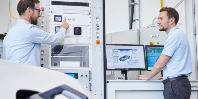
A smart charging station emulator from dSpace allows for the emulation of charging stations with a power of up to 85kW. According to dSpace, the emulator can accelerate the development of electric vehicles (EVs) for international markets.

The Smart Charging Station Emulator allows for the emulation of charging stations with a power of up to 85kW. Manufacturers of EVs and suppliers of battery systems can realistically test new developments with different technical charging standards and protocols, simulate a large number of faults, and develop them quickly and efficiently in line with the requirements of international markets, says dSpace.

It is based on dSpace’s Smart Charging Solution, which is used for testing onboard chargers, charging stations, and communication modules. Other components of the Smart Charging Station Emulator include a Scalexio real-time simulator, a dynamic and expandable model that runs on the simulator. There is also a power supply that enables DC charging and discharging at a maximum of 85kW. This means that vehicle-to-grid (V2G) scenarios can also be simulated, confirms dSpace.

All components are contained in a robust rack, fitted with wheels, to make the system flexible and mobile. It can be used not only in the laboratory but also for tests on prototype vehicles in workshops. There is automatic cable recognition, connecting communication and charge release, insulation monitoring and emergency stop switches, for operator safety.

The system supports international standards for charging communication such as ISO 15118 and DIN SPEC 70121, GB/T 27930, GB/T 18487, and CHAdeMO, and emulates a variety of charging stations and charging scenarios in real time. New charging standards such as CHAdeMO 3.0 or ChaoJi can be implemented.

The Smart Charging Station Emulator supports AC charging up to 63A and DC charging up to a maximum of 200A or 85kW. It is also adaptable to customer-specific charging supply requirements. In addition, the system offers almost unlimited options for manipulating electrical parameters and communication.

dSpace provides simulation and test solutions for developing networked, autonomous, and electrically powered vehicles. Automotive manufacturers and their suppliers use the company’s end-to-end solution range to test the software and hardware components of new vehicles long before a new model is allowed on the road.

As well as a partner for vehicle development, engineers in aerospace and industrial automation fields also rely on dSpace. The company’s portfolio ranges from end-to-end solutions for simulation and validation to engineering and consulting services as well as training and support.

Headquartered in Paderborn, Germany, dSpace has three project centres in Germany and serves customers through regional dSpace companies in the USA, the UK, France, Japan, China, and Croatia.

http://www.dspace.de

> Read More

Bridgetek’s evaluation hardware uses EVE technology for HMI prototypes

To assist with the initial development and prototyping of human machine interfaces (HMIs) based on Bridgetek’s object-oriented graphic controller ICs, the ME817EV evaluation board features Bridgetek’s BT817 embedded video engine (EVE) device. It allows engineers to experiment with the latest generation of EVE technology and its capabilities. The BT817 supports higher resolutions and large format displays to develop HMIs with broad functionality, offering greater visual clarity and enhanced video playback capabilities.

Measuring 165 x 100mm, the ME817EV has all the necessary attributes for undertaking development work relating to the graphics, audio and touch elements of the HMI. As well as audio amplification and multi-stage audio filtering features, an LED driver can be used to adjust the display backlighting. The evaluation board also includes a touch controller that supports five simultaneous touch points, with 16Mbytes of on-board flash memory resource for storing unicode fonts and image libraries.

The ME817EV can interface with large scale, high resolution display modules. For 1280 x 800 pixel displays it can connect through a 40-pin LVDS interface. A 50-pin RGB interface can be used for 1024 x 600 pixel displays. Capacitive touchscreens may be connected using a six- or 10-pin FPC connector. The board can be powered via a 5.0V supply using the SPI host connector, or via the USB Type-C port.

Fred Dart, founder and CEO of Bridgetek explains the company’s thinking behind this latest introduction: “It is clear that there is a real need for a more streamlined approach to larger format HMI construction. By providing this evaluation platform, we are making the whole project development process a lot quicker and easier for engineers to complete, with much better end results being derived too”.

Founded in 2016, Bridgetek supplies highly advanced ICs and board level products to meet the demands of a constantly evolving global technology landscape. The company’s Embedded Video Engine (EVE) graphic controller ICs each integrate display, audio and touch functionality onto a single chip. The EVE graphic controller ICs are complemented by its highly-differentiated, speed-optimised microcontrollers with augmented connectivity features.

http://www.brtchip.com

> Read More

First IP for PCI Express 6.0 has low latency for HPC and AI

IP that supports the latest features in the PCI Express (PCIe) 6.0 specification has been released by Synopsys. The DesignWare IP can be used for early SoC development, high performance computing and artificial intelligence (AI).

The IP for PCIe 6.0 includes controller, PHY and verification IP, for early development of PCIe 6.0 SoCs. It supports the latest features in the standard specification including, 64 GT/s PAM-4 signalling, FLIT mode and L0p power state. Acccording to Synopsys the IP addresses evolving latency, bandwidth and power-efficiency requirements of high performance computing (HPC), AI and storage SoCs.

To achieve the lowest latency with maximum throughput for all transfer sizes, the DesignWare Controller for PCI Express 6.0 uses a MultiStream architecture, delivering up to x2 the performance of a single-stream design. The controller, with available 1024bit architecture, allows designers to achieve 64Gtransfers per second x16 bandwidth and closing timing of 1GHz. The controller provides optimal flow with multiple data sources and in multi-virtual channel implementations. To facilitate accelerated testbench development with built-in verification plan, sequences and functional coverage, the VC Verification IP for PCIe uses native SystemVerilog/UVM architecture that can be integrated, configured and customised.

Synopsys’ DesignWare PHY IP for PCIe 6.0 provides adaptive DSP algorithms that optimise analogue and digital equalisation to maximise power efficiency regardless of the channel. The PHY enables near zero link downtime using patent-pending diagnostic features. The placement-aware architecture of the DesignWare PHY IP for PCIe 6.0 minimises package crosstalk and allows dense SoC integration for x16 links, added Synopsys. The datapath is optimised with ADC-based architecture for low latency.

The DesignWare Controller and PHY IP for PCIe 6.0 early access are scheduled to be available in Q3 of 2021. The Verification IP for PCIe 6.0 is available now.

Synopsys develops silicon-proven IP for SoC designs. The DesignWare IP portfolio includes logic libraries, embedded memories, PVT sensors, embedded test, analogue IP, wired and wireless interface IP, security IP, embedded processors and sub-systems. Synopsys’ IP Accelerated initiative offers IP prototyping kits, IP software development kits and IP subsystems accelerate prototyping, software development and integration of IP into SoCs. The company’s invests in IP quality, comprehensive technical support and robust IP development methodology to enable designers to reduce integration risk and accelerate time-to-market.

Image credit- iStock,DKosig

https://www.synopsys.com

> Read More

Microchip introduces software-based redundancy to network timing

With the introduction of the TimeProvider 4100 release 2.2 Grandmaster, Microchip provides a new level of software-based redundancy for the IEEE 1588 precise timing grandmaster with gateway clock.

It is intended for critical infrastructure providers, e.g. 5G wireless networks, smart grids, data centres, cable and transportation services, which require redundant, resilient and secure precise timing and synchronisation solution, explained Microchip.

In addition to the redundancy architecture, the TimeProvider 4100 Release 2.2 grandmaster has support for a multi-band global navigation satellite system (GNSS) receiver and enhanced security to ensure always-on precise timing and synchronisation.

Redundancy ensures uninterrupted services. Infrastructure deployments previously relied on hardware redundancy to avoid service disruption but the modular architectures are expensive. The TimeProvider 4100 Release 2.2 grandmaster provides redundancy via software implementation, enabling flexible deployment and lower hardware costs without sacrificing ports, pointed out Microchip.

It also introduces an increased level of resiliency by supporting a new GNSS multi-band, multi-constellation receiver to protect against time delay resulting from space weather, solar events and other disruptions that may impact critical infrastructure services. Multi-band GNSS is particularly important for the highest levels of accuracy including primary reference time clock Class B (PRTC-B) (40 nano seconds) and enhanced primary reference time clock (ePRTC) (30 nano seconds).

The TimeProvider 4100 Release 2.2 grandmaster also adds support for Radius and TACACS+ and also introduces anti-jamming and anti-spoofing capabilities.

In addition, the TimeProvider 4100 Release 2.2 grandmaster provides a super oven controlled crystal oscillator (OCXO) option for enhanced holdover capabilities in case of GNSS disruption.

The TimeProvider 4100 Release 2.2 grandmaster is a family of products with hardware expansion modules for legacy fan-out or Ethernet fan-out with 10Gigabit Ethernet support. It can be configured in specific operation modes to act either as a gateway clock, a high-performance boundary clock or an ePRTC.

The TimeProvider 4100 Release 2.2 grandmaster embeds additional Microchip technology including its OCXO, super OCXO, Rubidium atomic clock, field programmable gate arrays (FPGAs), Ethernet switch, synthesisers and cleaning oscillators.

The TimeProvider 4100 is part of Microchip’s virtual Primary Reference Time Clock (vPRTC) product portfolio, offering end-to-end precise time and synchronisation. The portfolio also includes Cesium atomic clocks for source of frequency and time, the BlueSky GNSS firewall for security, TimeProvider 4100 high-performance boundary clock and TimeProvider 4100 gateway clocks, as well as the TimePictra software suite, which manages the end-to-end precise time architecture across all Microchip timing products.

Microchip’s TimeProvider 4100 Release 2.2 grandmaster offers several options for software and hardware support including installation, sync audits, network engineering and 24/7 worldwide support.

The TimeProvider 4100 Release 2.2 grandmaster is available now for both new and already-deployed systems.

http://www.microchip.com

> Read More

About Smart Cities

This news story is brought to you by smartcitieselectronics.com, the specialist site dedicated to delivering information about what’s new in the Smart City Electronics industry, with daily news updates, new products and industry news. To stay up-to-date, register to receive our weekly newsletters and keep yourself informed on the latest technology news and new products from around the globe. Simply click this link to register here: Smart Cities Registration