Wi-Fi module is secure for WPA2 and WPA3-Personal Wi-Fi standards

Supporting the latest standards for secure networking, the PAN9520 2.4GHz 802.11b/g/n embedded Wi‑Fi module provides all the security features required for compliance with WPA2 and WPA3-Personal Wi-Fi security standards, says Panasonic Industry.

The PAN9520 is based on the Espressif ESP32-S2 microcontroller, which includes a high-performance 32-bit Xtensa LX7 CPU, a high sensitivity wireless radio, a baseband processor, boot loader and 320kbytes of SRAM. An encryption unit supports a range of security and encryption protocols, including CCMP, TKIP, WAPI, WEP, BIP, and AES.

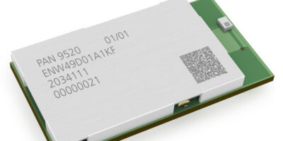
It includes flash memory, a 40MHz crystal oscillator and a chip antenna. The integrated crystal is claimed to ensure connection performance over the entire temperature range and lifetime. Although believed to be one of the smallest modules on the market, it offers a rich set of peripherals, including full-speed USB OTG, SPI, UART, I²C.

The integrated module can be implemented quickly and easily into end-product designs – with or without a host controller, says the company. Panasonic Industry offers two variants with either 2Mbyte PSRAM and 4Mbyte flash or no PSRAM and 1Mbyte flash.

The module supports access point mode and station mode in parallel, allowing simultaneous Wi-Fi connections to smart devices and home network routers.

There is also the Espressif IoT integrated development framework (ESP-IDF), with which engineers can develop software for a range of applications, and access software examples which can be used to speed up development.

Panasonic develops technologies for wide-ranging applications in the consumer electronics, housing, automotive, and B2B sectors. The company celebrated its 100th anniversary in 2018 and operates 528 subsidiaries and 72 associated companies worldwide.

Panasonic Industry Europe is part of the global Panasonic Group and provides automotive and industrial products and services in Europe. It researches, develops, manufactures and supplies technologies and has a portfolio which covers key electronic components, devices and modules up to complete solutions and production equipment for manufacturing lines across a broad range of industries.

http://industry.panasonic.eu

> Read More

Fusion Design platform enables first-pass silicon for Armv9-based SoCs

Multiple SoC tape-outs at early adopters of the Arm Cortex-X2, Cortex-A710, and Cortex-A510 CPUs based on Arm’s Armv9 architecture, Arm Mali-G710 GPUs and Arm DynamIQ Shared Unit-110, have been announced. They were achieved using Synopsys’ EDA and IP, including Fusion Design Verification Continuum and DesignWare Interface IP.

The latest SoCs, developed for high end consumer devices, use Armv9’s performance and power efficiency enhancements and jointly developed flows and methodologies targeting the latest 5nm, 4nm and 3nm process technologies.

The EDA tools and IP provide designers with the leading, SoC-centric, and power-first software-to-silicon solution, says Synopsys, to hasten the achievement of the maximum performance per Watt across various use cases, including specialised artificial intelligence (AI), digital signal processing (DSP) and virtual and augmented reality (XR) workloads which are expected to be broadly deployed in next generation consumer devices.

“Based on the Armv9 architecture, the Arm Total Compute solution is designed to deliver a step-change in compute performance and efficiency while providing the levels of native security and trust needed in an increasingly data-centric and connected world,” said Paul Williamson, senior vice president and general manager, Client Line of Business, Arm.

Designers creating Armv9-based SoCs for a range of markets, including smartphones, laptops, PCs, digital TVs, wearables, and augmented- and virtual-reality applications, select Synopsys’ portfolio of integrated digital, verification and interface IP solutions to achieve optimum differentiation and the fastest time-to-market, says the company.

“Data is becoming an ever-increasing and important currency in this knowledge-driven world, and its timely, efficient and secure processing is paramount in shaping a safe, information-leveraged future,” said Shankar Krishnamoorthy, general manager of the Digital Design Group at Synopsys. “Our broad portfolio of optimised design, verification, IP, software security and software quality solutions have been aggressively co-optimised with Arm to enable a new wave of high-value applications based on the Armv9 architecture, establishing the new benchmark for trustworthy, power-centric performance.”

According to Synopsys, the Fusion Design Platform delivers unprecedented full-flow quality-of-results and time-to-results. Fusion Technology redefines conventional EDA tool boundaries – test, synthesis, place-and-route, and signoff – by sharing common, best-in-class engines, enabling broad-flow optimisations and wide-ranging margin reduction for performance per Watt and time to results.

Early adopters of Arm’s Armv9 mobile solution are using Synopsys’ Verification Continuum Platform solutions optimised for Arm, including Virtualizer Development Kit (VDK) with Arm Fast Models for Cortex-X2, Cortex-A710, Cortex-A510 CPUs and Mali-G710 GPUs, VCS simulation, Verdi for hardware and software debug, Verification IP for the latest Arm AMBA interconnect, ZeBu Server and HAPS hardware to accelerate hardware-software development and power and performance validation to reduce time-to-market.

The DesignWare Interface IP portfolio provides the performance, power efficiency, security and real-time connectivity for Arm-based systems implementing the latest Cortex CPUs and Mali GPUs. Synopsys’ IP portfolio of controllers and PHYs supporting the latest protocols such as PCI Express, DDR, MIPI and USB, is optimised for the rapid development of Arm-based SoCs.

Synopsys QuickStart Implementation Kits (QiKs) include implementation scripts and reference guides and enable early adopters to accelerate time-to-market and achieve their demanding performance per Watt targets.

http://www.synopsys.com

> Read More

Lattice enhances sensAI stack to simplify AI/ML deployment

Enhancements to the Lattice sensAI solution stack are designed to accelerate artificial intelligence / machine learning (AI/ML) application development on Lattice’s low power FPGAs. The company has added support for the Lattice Propel design environment for embedded processor-based development and the TensorFlow Lite deep-learning framework for on-device inferencing.

Support for the TensorFlow Lite framework reduces power consumption and increases data co-processing performance in AI/ML inferencing applications. TensorFlow Lite runs anywhere from two to 10 times faster on a Lattice FPGA than it does on an Arm Cortex-M4-based microcontroller, reports Lattice.

Another enhancement is the stack’s support for Lattice Propel environment’s GUI and command line tools to create, analyse, compile, and debug both the hardware and software design of an FPGA-based processor system. Even developers unfamiliar with FPGA design can use the tool’s drag and drop interface to create AI/ML applications on low power Lattice FPGAs with support for RISC-V-based co-processing, claims Lattice.

Lattice sensAI Studio is a GUI-based tool for training, validating, and compiling ML models optimised for Lattice FPGAs.

The Lattice sensAI Studio design environment is for end-to-end ML model training, validation, and compilation. Developers can implement sensAI 4.0 using a simple drag and drop interface to build FPGA designs with a RISC-V processor and a convolutional neural network (CNN) acceleration engine to quickly implement ML applications on power-constrained edge devices.

Leveraging advances in ML model compression and pruning, sensAI 4.0 can support image processing at 60 frames per second with QVGA resolution or 30 frames per second with VGA resolution.

Lattice has also responded to the demand in multiple end markets to add support for low power AI/ML inferencing for applications like object detection and classification. AI/ML models can be trained to support applications for a range of devices that require low power operation at the edge, including security and surveillance cameras, industrial robots, and consumer robotics and toys. The sensAI solution stack helps developers rapidly create AI/ML applications that run on flexible, low power Lattice FPGAs, says the company.

http://www.latticesemi.com

> Read More

Configurable DeviceOn Module reduces wireless sensor development time

Enabling instant sensor to cloud connectivity, the WISE-1510-DOM DeviceOn Module is a certified wireless module in a compact industry-standard form factor. It is ready to use with no programming required, says Advantech Europe.

The DeviceOn Module family of modules is a combination of hardware modules and smart device firmware, delivered ready to use, for rapid deployment of custom or semi custom sensors.

This modular approach for smart sensors means that sensor OEMs can concentrate on their core business around the sensing technology, while leveraging Advantech’s capabilities in data transformation and transfer, explains the company. The DOMs can be used in smart waste management, smart street lighting, smart agriculture, asset tracking and cold chain/refrigerator monitoring.

The WISE-1510-DOM DeviceOn Module measures 22 x 30mm and is M2.COM-compliant. The module that contains a wireless modem, MHF4 antenna connector, Arm Cortex-M4 processor and I/O interfaces for sensors. The module is ready to be used on either standard Advantech or custom carrier boards. Wireless connectivity and sensor interfaces can be configured through a graphical user interface (GUI).

Sensor designers can integrate LoRaWAN long-range connectivity into devices. The WISE-1510-DOM module consumes low-power in transmit and receive modes, and has a deep-sleep mode drawing just 36 microA. Variants supporting cellular NB-IoT/LTE-M, Bluetooth, Wi-Fi and other standards will become available soon advises Advantech.

Advantech’s WISE-DeviceOn firmware is integrated in the module, providing software functionality to interface with a range of supported sensors, permitting dynamic sensor configuration like names and thresholds, sensor and event handling as well as data caching. Multiple interfaces are provided for sensor and I/O control, including one UART (optional), general purpose I/Os (GPIOs), four ADC channels, PWM, SPI, and I2C. Configuration or firmware updates can simply be performed via USB.

The DeviceOn server layer can be hosted on any platform, Advantech provides default integrations for Microsoft Azure and Advantech’s cloud platform, WISE-PaaS/EnSaaS, as well as interfaces to other cloud platforms such as Google or AWS, and on premise support, utilising a company’s own IT infrastructure or dedicated DeviceOn server hardware from Advantech.

Advantech also offers three compatible DeviceOn Module sensor boards, the DOM-SB-001 for temperature, humidity, and brightness sensing, the DOM-SB-003 with a brightness sensor and a time-of-flight proximity and ranging sensor, and the DOM-SB-004 for air-quality and brightness sensing.

An evaluation kit is available, in three formats. There is a board-only option, a board with an enclosure, or a board with an enclosure and a WISE-6610-E100-A LoRaWAN gateway allowing scalability up to 100 nodes.

http://www.advantech.eu

> Read More

About Smart Cities

This news story is brought to you by smartcitieselectronics.com, the specialist site dedicated to delivering information about what’s new in the Smart City Electronics industry, with daily news updates, new products and industry news. To stay up-to-date, register to receive our weekly newsletters and keep yourself informed on the latest technology news and new products from around the globe. Simply click this link to register here: Smart Cities Registration