Sensor evaluation board accelerates IoT development, says Bosch Sensortec

R&D effort can be simplified to assist rapid prototyping and reduce time to market for the segmented IoT market, using the Application Board 3.0, says Bosch Sensortec. It offers Bluetooth connectivity and a small form factor for IoT applications and supports the full range of Bosch Sensortec sensors

The Application Board 3.0 simplifies the evaluation and prototyping of sensors for a wide range of applications, particularly in Industry 4.0, IoT, smart home systems, and wrist- and head-mounted wearables, explained Bosch-Sensortec.

Any Bosch Sensortec sensor mounted on a ‘shuttle board’ is simply plugged into the socket on the Application Board. All shuttle boards have an identical footprint, and Bosch Sensortec’s software automatically detects which sensor is plugged in at any given moment to launch the appropriate software. This enables the straightforward evaluation of a wide range of sensors and solutions, said Bosch Sensortec. Prototypes can be built to quickly test different use case configurations, added the company.

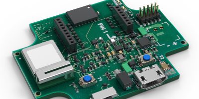
 The board measures just 47.0 x 37.0 x 7.0mm3, which is practical for evaluating sensors used in portable applications, observed Bosch Sensortec. The board can be powered using a 3.7V Li-ion battery or a standard 5V USB power supply.

“The Application Board 3.0 makes it quick and easy for developers to build their projects with any of our sensors on a single platform, meaning that they can now focus on creating unique use cases and differentiating their products,” says Dr. Stefan Finkbeiner, CEO at Bosch Sensortec. “Our customers also benefit from efficient support through regional field application engineers and Bosch offices,” he continued.

The integrated development environment (IDE) software provided with the board includes a simplified graphical user interface (GUI) to evaluate and tune sensor parameters, as well as to visualise and record sensor data. The software also saves time in troubleshooting sensor-related issues, claims Bosch Sensortec.

Application Board 3.0 is designed around the u-blox NINA-B302 Bluetooth Low Energy (BLE) module and is based on the nRF52840 chipset from Nordic Semiconductor, which includes an Arm Cortex-M4F CPU. It is certified and compliant with multiple directives for different international regions: CE, RoHS, China RoHS, FCC, IC, VCCI, SRRC and NCC.

The board is supplied with 256kbyte RAM, 1Mbyte of internal flash and 2Gbyte of external flash memory for data logging. It provides full-speed micro-USB 2.0 connectivity and BLE to connect to a host, such as a PC, for transferring the logged sensor data from the board.

The Application Board 3.0 is available now.

http://www.bosch-sensortec.com

> Read More

Imec develops 120Gbaud SiGe BiCMOS to advance optical interconnects

To enable a “significant increase” in baud rate combined with at least 80GHz analogue output bandwidth, a scalable SiGe BiCMOS technology developed by Imec, can be produced in volume, “paving the way to cost-effective, high-speed optical transceivers for the Tbit era,” said the research group.

It has been designed for data-intensive applications, such as cloud services, video streaming, high-performance computing and 5G, which place demands on optical communication networks within data centres. The most performant optical links operate at speeds up to 400Gbits per second, using for example four 100Gbit per second channels. Data centre operators believe that Terabit per second optical transceivers will be needed within a few years. At the same time as the increasing demands on data centres’ optical networks, co-packaged paradigms are emerging to help optical switches manage the massive bandwidth density at input. These are also expected to reach 100Terabits per second. In these co-packaged optics, Si photonics transceivers are tightly integrated with the high-speed electronic circuits.

Increasing the capacity of the optical links despite the smaller footprints of transceivers will impact the design of photonic high-speed ICs used in transceivers, said Imec. One solutions is to increase signalling rates beyond 100Gbaud. Such rates may be beyond the capabilities of advanced CMOS nodes (for example FinFETs), leaving greater than 100Gbaud speeds to be handled by InP technologies, where their smaller wafer sizes and reduced capability to integrate more complex functionality makes scaling up these processes challenging. Imec is looking at III-V on CMOS processes, initially with the integration of novel circuit architectures in SiGe BiCMOS to achieve beyond 100Gbaud operation.

Scientists from imec-IDLab have developed a novel transmitter architecture that has key building blocks fabricated in a mainstream SiGe BiCMOS process. Imec’s Peter Ossieur, explained: “The resulting IC decodes four 30Gbaud PAM-4 (or four 60Gbits per second NRZ) streams, and simultaneously multiplexes and equalises these streams into a 120Gbaud PAM-4 signal with more than 80GHz bandwidth, 1.2Vpp voltage swing and 2200mW power consumption. Since the four-level pulse amplitude PAM-4 modulation format involves two bits per symbol (denoted as 00, 01, 10 and 11), this is the equivalent of a 240Gbit per second (single lane) transmitter, he told Electronic Design.

Within the transmitter IC, a multiplexer (MUX) combines multiple low-speed input signals from a CPU or GPU within the data centre, into a single full-rate data stream. This stream is then equalised to compensate for any bandwidth losses in the modulator and the channel. The high-speed equalised signal is then used as an input signal for the driver that subsequently feeds the optical modulator.

Rather than performing equalisation in the digital domain using a DSP, before conversion into an analogue signal, Imec has developed a transmitter IC architecture which implements an analogue signal processing variant of the DSP filter, with the integrated MUX, FFE and driver fabricated in mainstream 55nm SiGe BiCMOS.

“The work shows a doubling of the operating rate compared to FinFET solutions and closely matches the speed and power obtained in InP-based solutions”, reported Peter Ossieur.

“These building blocks will also be crucial for developing novel coherent transceiver concepts, which exploit the phase and polarisation of the optical field to further increase the bit rate,” said Ossieur.

http://www.imec-int.com

> Read More

Intuitive GNSS receiver evaluation software gives GPS a boost

Global navigation satellite system (GNSS) evaluation software from u-blox, u-center 2, offers advanced features to explore u-blox positioning technologies.

The software runs on Microsoft Windows and is suitable for 10 generation u-blox GNSS technology. It has an intuitive interface to configure GNSS products, evaluate their performance, improve software quality and experience the performance boost achieved using GNSS-related services, said u-blox.

The successor to the u-blox u-center GNSS evaluation software is compatible with the latest u-blox M10 GNSS technology. u-center 2 includes additional features which simplify the configuration, evaluation, and software development of GNSS-based solutions.

It provides personalised workspaces with adaptive windows for a choice of views to observe the connected GNSS receiver’s static and dynamic behaviour. A built-in log player accepts log files from the previous version of the software. It also features  message- and time-based navigation and lets users set the playback speed. Updates are automatic to ensure that the software always includes the latest features, added u-blox.

It also serves to simplify the evaluation of GNSS-related location services, including AssistNow, through which GNSS receivers gain access to GNSS aiding data, enhancing startup performance and saving power, claimed the company.

Bernd Heidtmann, product manager, product strategy for Standard Precision GNSS at u-blox, commented: “With its fresh and minimalist user interface, the upcoming quick product configuration designed for key use cases, and optimised data logging, u-center 2 will raise the benchmark for GNSS evaluation tools in terms of performance and user experience.”

u-center 2 is free for download.

u-blox specialises in positioning and wireless communication in automotive, industrial, and consumer markets, providing services and products which let people, vehicles, and machines determine their precise position and communicate wirelessly over cellular and short range networks.

The company’s portfolio of chips, modules, and secure data services and connectivity, allows customers to develop solutions for the IoT, quickly and cost effectively.

The company’s headquarters are in Thalwil, Switzerland, with offices in Europe, Asia, and the USA.

http://www.u-blox.com

> Read More

Compact, low noise oscillators perform for data centres

The ProXO+ family of compact, low noise, temperature-controlled clock oscillators from Renesas are high frequency, differential oscillators suited to fibre optic transceiver modules, accelerator cards, smart NIC cards, and networking equipment applications.

“The ProXO+ family delivers on all counts, offering tight frequency stability, great jitter performance, and high output frequency, which are critical features for communications, cloud and compute markets,” said Bobby Matinpour, vice president of timing products at Renesas. The level of programmability also enables the use of a single device for numerous designs, simplifying the bill of materials (BoM), sourcing and inventory management, he added.

The oscillators have a frequency stability ±3 parts per million (ppm) from -40 to +85 degrees C and programmable frequencies up to 2.1GHz. They exhibit 135fs typical phase jitter at 12kHz to 20MHz range.

The ProXO+ devices are available now for order in an eight-pin plastic package measuring 3.2 x 2.5mm.

Renesas also announced two industry-standard plastic packages for its existing ProXO XF 2.5 x 2.0mm oscillators. They are now also available in 3.2 x 2.5mm and 5.0 x 3.2mm packages.

The ProXO+ family can be combined with Renesas’ complementary clock buffers, power devices and microcontrollers, such as the Xilinx Kintex-7 Power and Timing, the CC-Link IE TSN, and the System on Module (SoM) with RZ/G2E. Renesas’

Renesas claims to provide the industry’s broadest timing portfolio to support the complete clock tree. It describes itself as a “one-stop-shop” for timing solutions, offering expertise and products from full-featured system solutions to simple clock tree building-block devices.

Renesas Electronics delivers embedded design innovation with complete semiconductor solutions that enable billions of connected, intelligent devices. Its portfolio of microcontrollers, analogue, power, and SoC products is available for a broad range of automotive, industrial, Infrastructure, and IoT applications.

http://www.renesas.com

> Read More

About Smart Cities

This news story is brought to you by smartcitieselectronics.com, the specialist site dedicated to delivering information about what’s new in the Smart City Electronics industry, with daily news updates, new products and industry news. To stay up-to-date, register to receive our weekly newsletters and keep yourself informed on the latest technology news and new products from around the globe. Simply click this link to register here: Smart Cities Registration