ToF sensor with multiple sensing zones elevates automation

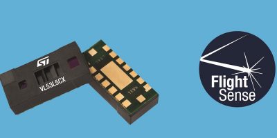
Distance sensing takes on new scope with the first multi-zone FlightSense time of flight (ToF) sensor from STMicroelectronics. The VL535CX also has up to 64 sensing zones (8×8) and can be used gesture recognition and complex scene analysis as well as for general purpose applications in the consumer and industrial markets.

The VL53L5CX’s multiple sensing zones offer multi-target detection, distance measurement up to four meters in each zone, and a wide square-edged field of view with 63 degrees diagonal. The sensor can be used for gesture recognition and complex scene analysis including 3D room mapping for robotics, storage-tank level monitoring to assist in inventory management, liquid-level control, and waste-bin-level monitoring used in smart refuse collection.

By supporting gesture recognition and automatic human-presence detection, the VL53L5CX enables safe, touch-free operation and saves power when used for waking-up publicly accessible equipment such as self-service payment terminals, and a variety of IoT-enabled, smart consumer products and domestic appliances. The sensor uses ST’s proven histogram processing which reduces the impact of cover-glass crosstalk. As a result, the sensor can be integrated and hidden behind front panels. A motion-indicator allows the sensor to detect if the target has moved or not.

The number of sensing arrays is programmable and the sensor can provide up to 60 frames per second in 16-zone (4×4) mode for fast-ranging mode. Simple software configuration enables it to reach high resolution of 8×8 zones. This is particularly useful to assist keystone correction for video projectors, for example, and provides a mini depth-map for augmented reality and virtual reality (AR / VR) applications.

The VL53L5CX contains a low power microcontroller and is capable of autonomous operation to conserve energy in power-saving applications. It is supplied in an integrated 6.4 x 3.0 x 1.5mm module that contains an infra red vertical cavity surface emission laser (VCSEL) emitter and a receiver with embedded single-photon avalanche diode (SPAD) and histogram-based ToF processing engine.

For prototyping, ST provides an evaluation and calibration tool. Development boards designed to integrate easily into larger prototype systems are also available. There is also the P-NUCLEO-53L5A1 evaluation kit and X-CUBE-TOF1 software expansion pack to develop ToF applications.

All parts are in production now.

http://www.st.com

> Read More

Australis eFPGA IP tool for rapid prototyping is built on OpenFPGA framework

Rapid prototyping of customisable FPGA architectures is automated with the latest tool from QuickLogic. The Australis embedded FPGA (eFPGA) IP Generator integrates QuickLogic’s best practices for performance, power, and area optimisation, said the company, to ensure low risk and low cost for eFPGA IP licensees

Its automation capability enables custom-parameterised eFPGA IP is available rapidly – within days in some cases, said the company.

Interest in domain-specific devices has been increased as the industry faces severe semiconductor supply constraints and difficulties keeping up with Moore’s Law, said QuickLogic. This is typically an expensive course for system developers and they may take longer to develop and may introduce risk. Integrating embedded FPGA technology can mitigate these risk but the fact that they are conventionally tied to a particular foundry and process node can deter developers. QuickLogic says Australis addresses these issues by giving developers the ability to customise eFPGA IP quickly and cost- effectively.

It is based on the OpenFPGA IP generator and adds additional features and capabilities specific to implementing QuickLogic’s eFPGA IP, along with testing and support required to build commercially-viable eFPGA IP.

It can provide ASIC/SoC developers a highly automated way to define and implement customised eFPGA IP. Embedded FPGA enables reprogrammable use, so that devices can address changing market conditions, support the evolution of new standards with the same silicon, customise implementations for IP protection, offload and accelerate hardware for artificial intelligence / machine learning  (AI / ML) or it can be used to create a range of product variants for small, niche or fragmented markets.

Australis provides customised eFPGA IP, from description to GDSII format in days and can meet specific Soc design requirements, such as being optimised for power, performance and area requirements.

According to QuickLogic, IP is a fraction of the cost of traditionally-built eFPGA IP cores.

In addition, a broad range of foundries and processes is supported, so developers can choose the best fab and technology for a given application.

ASIC / SoC and FPGA user tool support ensure seamless integration of the IP, continued QuickLogic.

The Australis eFPGA IP Generator is available now.

QuickLogic is a fabless semiconductor company that develops low power, multi-core semiconductor platforms and IP for artificial intelligence (AI), voice and sensor processing. The company offers embedded FPGA IP (eFPGA) for hardware acceleration and pre-processing, and heterogeneous multi-core SoCs that integrate eFPGA with other processors and peripherals. There is also the Analytics Toolkit, following the acquisition of SensiML, offering sensor algorithms using AI technology. Markets served include AI, voice, and sensor processing across mobile, wearable, hearable, consumer, industrial, edge and endpoint IoT.

https://www.quicklogic.com

> Read More

Renesas adds GUI and design parameters to Lab on the Cloud environment

Testing for voice and mobile applications are design parameters that Renesas Electronics has added to its Lab on the Cloud environment to simplify configuration and testing, while accelerating time to market.

The Lab on the Cloud environment enables customers to remotely access, configure, test, monitor and measure Renesas products instantly 24/7 in a cloud-connected lab. There, users can find evaluation boards for popular devices, together with proof of concept boards from Renesas and its partners. Users can access the physical lab through a PC-based graphics user interface (GUI) that enables them to immediately begin configuring and testing designs without requiring a physical board.

The GUI introduces parameters for control and additional results for monitoring. The ergonomic lab layout combined with an intuitive user interface have been designed to make it easier for users to quickly navigate the environment, said Renesas. For instance, the centralised live camera feed gives users a view of the complete lab set up and results; it also has the ability to zoom in and out on real time testing and data capture readings.

There are advanced implementations in test set ups and control for voice recognition, mobile application and power supply which enable users to complete complex testing such as transient performance in a few mouse clicks, Renesas continued.

New options include the Femtoclock2 point of use timing devices, which is claimed to be the smallest and lowest power clock generation and jitter attenuation device available, at less than 100fs.

Developers can test these and other devices via Lab On the Cloud to ensure stringent performance requirements are met, as well accelerating time to market.

New sections in the Lab on the Cloud suite including timing, power supply, voice recognition and control, healthcare, safety and surveillance, industrial communication, and IEEE 1588/5G computing and communication.

There are also a further 14 evaluation boards that have been added to the Lab on the Cloud environment, bringing the total to 23, covering IoT battery systems, industrial CAN sensor networks, voice recognition, air quality and capacitive liquid level indication, surveillance camera with CMOS sensor and a super capacitor-based terminal back up  power supply.

According to Renesas the enhancements of an advanced GUI and new design parameters create a more engaging and ergonomic user experience, and offer designers greater configuration flexibility.

http://www.renesas.com

> Read More

Toshiba adds 20 microcontrollers to TXZ+ family for high speed data processing

Toshiba Electronics Europe has added 20 microcontrollers to its TXZ+ family. The M4G group microcontrollers use Arm Cortex-M4 microcontrollers for data processing and are manufactured using a 40nm process.

The microcontrollers, in common with existing TXZ+ devices can be used for high speed data processing applications, for example in IoT equipment, building automation, factory automation, home appliances, AV equipment, multi-function printers and other office equipment.

In addition to the Arm Cortex-M4 core, the new microcontrollers include a floating point unit (FPU) that runs at speeds up to 200MHz. They also integrate 2048kbyte of flash memory for code, a further 32kbyte of data flash with 100k write cycles endurance and 4kbyte of user data flash. They also incorporate multiple interfaces and various communication options.

As with the other devices in the M4G group, the latest additions have enhanced communication functions integrated as a serial memory interface. Among the standards supported are quad / octal SPI, audio interface (I2S), UART, FUART, TSPI and I2C. A three-unit DMAC and bus matrix structure is claimed to “significantly” improve communication throughput, compared to conventional products.

The new microcontrollers have a high speed, high precision 12-bit ADC to support a variety of sensing applications. The ADC allows individual sample-and-hold times to be set for each input channel with up to 24 channels. If integrated with Toshiba’s advanced programmable motor driver (A-PMD), the devices can also be used in AC motor, brushless DC (BLDC) motors, said the company.

Self-diagnosis functions for ROM, RAM, ADC and the clock contribute to the devices’ IEC60730 Class B functional safety certification. The microcontrollers maintain good compatibility with devices within the existing TXZ family M4G group.

Comprehensive documentation, sample software (with examples of actual usage), and driver software for each peripheral are available for free download on the company’s website. Additionally, evaluation boards and development environments are provided in co-operation with Toshiba’s global ecosystem partners.

The new microcontroller products are in mass production now.

http://www.toshiba.semicon-storage.com

> Read More

About Smart Cities

This news story is brought to you by smartcitieselectronics.com, the specialist site dedicated to delivering information about what’s new in the Smart City Electronics industry, with daily news updates, new products and industry news. To stay up-to-date, register to receive our weekly newsletters and keep yourself informed on the latest technology news and new products from around the globe. Simply click this link to register here: Smart Cities Registration