TSN Ethernet switches are turnkey for industrial automation

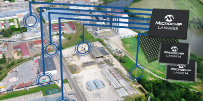
Believed to be the industry’s first turnkey devices for industrial automation networks, the Microchip’s LAN9668x family of time sensitive networking (TSN) switching devices delivers IEEE standards-compliant features to lower latency data traffic flows and greater clock accuracy.

Connected warehouses and other industrial ecosystems with converged IT and operational technology architectures rely on TSN and Ethernet for precise timing, synchronisation and connectivity of devices including cameras, barcode readers, scanners and conveyors. These ecosystems require next-generation network technology to interconnect device, sensor and equipment communication. The LAN9668 TSN switching devices deliver IEEE standards-compliant features and are complemented by Microchip’s LAN8814 quad-port Gigabit Ethernet (GbE) physical layer (PHY) transceiver. 

Microchip’s LAN9668-I / 9MX and LAN9668-9MX devices are eight-port switches for industrial and commercial applications, respectively, outfitted with Arm Cortex-A7 central processing units (CPUs), supporting TSN IEEE standards for communication in industrial settings. These include IEEE 1588v2 and IEEE 802.1AS-2020 for precision timing, IEEE 802.1Qci for per-stream filtering and policing, IEEE 802.1Qav and IEEE 802.1Qbv for traffic shaping and IEEE 802.1CB for seamless redundancy, as well as IEC-62439-2 (Media Redundancy Protocol) and ODVA-DLR and IEC-61158-6-10 for media redundancy. 

Microchip’s Ethernet Switch API (MESA) and PHY API (MEPA) enable designers to develop a comprehensive, user-friendly function library that is operating-system independent. The LAN9668 and LAN8814 scalable TSN chipsets are supported by Microchip’s software framework and provide the lowest latency and end-to-end transmission of communication traffic.

The LAN8814 is a quad-port GbE PHY that supports the latest TSN requirements including IEEE 1588 v2 and frame pre-emption. Designers using LAN9668 and LAN8814 technology can employ the TSN chipset to achieve timing, stream reservation, protection and management, to reduce both development time and cost.

“While devices and equipment previously required their own communication systems, TSN improves interoperability through connecting data streams to simplify traffic,” said Charles Forni, vice president of Microchip’s USB and networking business unit. “Enabling converged network architectures, this technology allows developers to expand their products into new markets and provide better performance in existing networks,” he added. 

Microchip also provides associated IStaX/SMBStaX and WebStaX network operating systems. They include a reproduceable reference design available as a board design or kit of Microchip parts including TSN switches, Ethernet PHYs, clock devices and oscillators. 

The LAN9668-I / 9MX and LAN9668-9MX TSN Ethernet switches are supported by the VSC6817SDK IStaX Linux application software, an industrial Ethernet switch software solution supporting Microchip’s managed Ethernet switch devices. The VSC6817SDK IStaX Linux network OS is an industrial Ethernet switch software which supports Microchip’s managed Ethernet switch devices. The SMBStaX Linux network OS and WebSTaX Linux network OS are available to commercial designers. These development tools are highly integrated with advanced L2+ switch features. 

Reference designs and evaluation boards also are available from Microchip and the company’s distribution partners.

The LAN9668/9MX and the LAN8814/ZMX are available in volume production.

http://www.microchip.com 

> Read More

Zener diodes prolong battery time and save PCB space

Low current regulator diodes are available from Nexperia in three surface mount package options. The 50 microA Zener diodes are available in three surface mountable package options: SOT23 (BZX8450), SOD323 (BZX38450) and SOD523 packages (BZX58550) and leadless DFN1006BD-2 (BZX8850S) package. 

They are also available as Q-portfolio parts, meeting the AEC-Q101 and ISO/TS16949 automotive quality standards. Nexperia explained that more non-automotive applications require additional quality-related services and extended longevity, and these needs will be met by these Q-portfolio parts. 

Specified at a low test current (50 microA), the efficient diodes are ideal for low bias and portable battery-powered devices in mobile, wearable, automotive and industrial applications.

“The DFN1006BD-2 packaged parts with side-wettable flanks (SWF) address the concerns of various sectors, such as size, performance and ruggedness, and match many diverse applications,” says Paula Stümer, product manager at Nexperia. 

There are 40 types per package option covering nominal working voltages from 1.8 to 75V. The Zener diodes feature a non-repetitive peak reverse power dissipation of up to or equal to 40W, total power dissipation up to or equal to 300mW and low dynamic resistance. 

The DFN package dimensions are 1.0 x 0.6 x 0.47mm and are suitable for replacing bulky leaded packages on PCBs. The package can save up to 60 per cent of real estate. It features side-wettable flanks (SWF), which ensure the solder flows up the side of the chip when it is soldered onto the PCB. This technology facilitates automated optical inspection (AOI), satisfying the automotive industry’s high safety, reliability and quality requirements. The high P(tot) of the DFN-packaged Zener diodes also run cooler than leaded parts, therefore improving system reliability.

The 50 microA Zener diodes are available as samples and in volume production quantities. 

Nexperia produces essential semiconductors, with an extensive portfolio which includes diodes, bipolar transistors, ESD protection devices, MOSFETs, GaN FETs and analogue and logic ICs. 

Nexperia, a subsidiary of Wingtech Technology Co., Ltd. (600745.SS), has an extensive IP portfolio and is certified to IATF 16949, ISO 9001, ISO 14001 and ISO 45001. It operates in Asia, Europe and the USA.

http://www.nexperia.com

> Read More

IP enables secure communications between chiplets

Secure die-to-die communication between chiplets can be achieved with the Fortrix SecureD2D IP, says CEVA. The IP enables secure authentication and firmware boot / code load between chiplets in a heterogeneous SoC (HSoC).

The cost of developing monolithic SoCs at advanced nodes has increased, and coupled with long design cycles and manufacturing lead times, this has led to the emergence of chiplets as a viable, cost-effective alternative, explains CEVA.

Security and assurance are key considerations for the adoption of HSoCs as the chiplet dies can originate from different vendors and different global supply chains. This is a key consideration for the deployment of chiplets in the aerospace and defence, industrial and automotive markets as well as in any IoT-related application where HSoCs are targeted. 

CEVA, through its wholly-owned subsidiary, Intrinsix, offers the Fortrix SecureD2D IP to enable secured communication between chiplets in an HSoC. 

The Fortrix SecureD2D IP consists of a controller communicating over a secure fabric to hardware-based crypto accelerators which perform rapid encryption and decryption to enable cryptographic functions such as ECDSA, SHA2 and AES. A low-level firmware API and a customisable high-level application allow rapid integration into secure chiplets and the IP implements both leader and follower termination points.

Fortrix SecureD2D IP is available for licensing today. Deliveries include RTL, SDC constraints, firmware and documentation. The IP is suitable for any semiconductor process, confirmed CEVA. The company also provides design services to help integrate and support the security IP and chiplet development in addition to full HSoC design and delivery. 

The IP was selected and deployed as part of the Department of Defense State-of-the-Art Heterogeneous Integrated Packaging (SHIP) program and has already been adopted by Lockheed Martin and a world-leading semiconductor company, reported CEVA.

CEVA is a licensor of wireless connectivity and smart sensing technologies and integrated IP. It provides DSPs, AI engines, wireless platforms, cryptography cores and complementary software for sensor fusion, image enhancement, computer vision, voice input and AI. These technologies are offered in combination with our Intrinsix IP integration services, to help customers address complex and time-critical IC design projects.  

The company’s DSP-based solutions include platforms for 5G baseband processing in mobile, IoT and infrastructure, advanced imaging and computer vision for any camera-enabled device, audio / voice / speech and low-power, always-on / sensing applications for multiple IoT markets. For sensor fusion, its Hillcrest Labs sensor processing technologies provide a range of sensor fusion software and inertial measurement units (IMUs) for markets including hearables, wearables, AR / VR, PCs, robotics, remote controls and the IoT. For wireless IoT, it supplies platforms for Bluetooth (low energy and dual mode), Wi-Fi 4/5/6/6E (802.11n/ac/ax), Ultra-wideband (UWB), NB-IoT and GNSS. 

http://www.ceva-dsp.com

> Read More

Interference waveform pattern software targets 5G and LTE testing

Tools which generate 3GPP interference waveform patterns for testing the receiver sensitivity and throughput of both 5G and LTE user equipment (UE) and modules using the Vector Signal Generator MG3710E are available from Anritsu.

Installing the Interference Waveform Pattern for 5G NR receiver test MX371055A and Interference Waveform Pattern for LTE receiver test MX371054A software in the MG3710E used in combination with the Radio Communication Test Station MT8000A and Radio Communication Analyzer MT8821C facilitates easy interference evaluation tests required by the 3GPP RF compliance test.

The tools are designed to support both in-house pre-testing for confirming compliance of Sub-6GHz 5G and LTE UE and modules before the official 3GPP compliance test as well as for R&D to improve receiver sensitivity and throughput performance.

Anritsu developed these two 3GPP-compliant interference waveform pattern tools to help engineers without specialist skills generate interference waveforms for easy interference tests.

In parallel with increasing 5G smartphone shipments, annual shipments of 5G customer premises equipment (CPE) are increasing based on mobile operator fixed wireless access (FWA) services. Manufacturers of automotive electronic equipment are developing 5G communications modules, such as the telematics control unit (TCU). Alongside the growing market for 5G UE and modules, the same manufacturers are developing LTE UE and modules for mobile operators who have not started 5G services yet.

Anritsu provides communications test and measurement solutions for 125 years. It helps customers develop wireless, optical, microwave / RF and digital solutions for R&D, manufacturing, installation and maintenance applications, as well as multi-dimensional service assurance solutions for network monitoring and optimisation. Anritsu also provides precision microwave / RF components, optical devices, and high-speed electrical devices for communication products and systems. The company develops advanced solutions for 5G, M2M, IoT, as well as other emerging and legacy wireline and wireless communication markets. 

http://www.anritsu.com 

> Read More

About Smart Cities

This news story is brought to you by smartcitieselectronics.com, the specialist site dedicated to delivering information about what’s new in the Smart City Electronics industry, with daily news updates, new products and industry news. To stay up-to-date, register to receive our weekly newsletters and keep yourself informed on the latest technology news and new products from around the globe. Simply click this link to register here: Smart Cities Registration