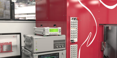
NXP integrates AES with EAL3+ for secure contactless MiFare

Claimed to be the most secure member of the MiFare Ultralight family, NXP Semiconductors has integrated Advanced Encryption Standard (AES) with Common Criteria EAL3+ security certification to enhance privacy and security in limited-use contactless tickets, RFID basic guest cards and other limited-use contactless applications.

MiFare Ultralight AES is for limited-use contactless tickets and cards, such as RFID basic guest cards, event tickets, access passes, loyalty cards or transit tickets. IT uses cryptography with sufficient key length recommended by the National Institute of Standards and Technology for secure authentication and protected data access and there is the option to limit negative authentication attempts. 

The ICs offer protected data access based on AES authentication with 128-bit key length and optional Command Counter to limit negative authentication attempts. They also have a configurable secure messaging communication mode with CMAC for integrity protection and a 7-byte UID with optional Random ID support for enhanced privacy. An ECC-based originality signature allows product validation based on public key (pre-programmed). The ICs include a 144-byte EEPROM and are ISO / IEC 14443 A -2 / -3 compliant.

The secure implementation is suitable for guest protection and secure room access or as a secure transport ticket in smart cities.  

Andre Perchthaler, segment manager, MiFare Smart Cities, at NXP, said: “By taking advantage of a single, standard-based encryption method, such as AES, service providers have the benefit of greater fraud prevention, while also being able to streamline integration and key management. With MiFare Ultralight AES, the full MiFare product portfolio now serves AES authentication from single-use up through multi-applications, simplifying access infrastructure, and reducing complexity and maintenance costs.”  

NXP Semiconductors claims to be the world leader in secure connectivity solutions for embedded applications, NXP is pushing boundaries in the automotive, industrial and IoT, mobile, and communication infrastructure markets. 

http://www.nxp.com

> Read More

Stella E MCUs power software-defined EVs

Automotive microcontrollers (MCUs) optimised for electric vehicles (EVs) and centralised (domain and zonal) electronic architectures have been released by STMicroelectronics. According to ST, they enable EVs to become more affordable, drive further and charge faster.

In current EVs, high-efficiency silicon carbide (SiC) -based power modules enable the greatest driving range and faster charging. Until now, they have required dedicated high-speed signal processors to control the advanced SiC power semiconductors. The Stellar E MCUs launched by ST are designed for the next generation of software-defined EVs, integrate high-speed control-loop processing on-chip. A single MCU can control the entire module, says ST, simplifying module design, saving costs and easing compliance with automotive safety and security standards.

The MCUs extend ST’s Arm-based Stellar family. They are a centralised domain and zone controller which simplify automotive electrical architectures for increased power, flexibility and safety, explained ST. 

The MCU family includes the Stellar P series for integration and vehicle control and the Stellar G series for body applications. The Stellar family architecture integrates multiple Arm Cortex cores that deliver high performance with the opportunity for lock-step redundancy and support real-time hardware virtualisation. All Stellar devices are designed for software upgradeability through secure over-the-air (OTA) updates.

The first product in the Stellar E series, the Stellar SR5E1 is optimised for EV on-board chargers (OBC) and general DC/DC converters, is now sampling to lead customers. Full production will begin in 2023. 

The Stellar E (Stellar Electrification MCUs) series are automotive-qualified MCUs that perform the high speed, control loop processing alongside general control in the same chip. 

The MCUs can control multiple power converters, leveraging features including a high speed ADC, a pulse-width modulation (PWM) controller and fast-acting protection circuitry.

The Stellar E series supports the leading automotive standards for functional safety (ISO 26262 ASIL-D), security (HSM -), and industry standard software interoperability (via Autosar 4.3.x), as well as secure OTA update. The Stellar family is supported with an extensive software-development toolchain with a common ecosystem for control and actuation.

http://www.st.com

> Read More

GaN FETs perform for e-bikes, drones and robotics, says EPC

Introducing the EPC9167 GaN-based inverter reference design, Efficient Power Conversion (EPC) said that the FET enhances motor system performance, range, precision and torque, while lowering overall system cost. 

The three-phase brushless DC (BLDC) motor drive inverter uses the EPC2065 eGaN FET. The EPC9167 operates from an input supply voltage between 14 and 60V (nominal 48V) and is available in two configurations – a standard unit and a high current version.

The EPC9167 standard reference design board is a three-phase BLDC motor drive inverter board featuring the EPC2065 eGaN FET rated at 3.6 mOhm maximum RDS(on), 80V maximum device voltage. This standard configuration uses single FETs for each switch position and can deliver up to 20A RMS maximum output current.

For the high current configuration, the EPC9167HC, reference design uses two paralleled FETs per switch position with the ability to deliver up to 42Apk (30A RMS) maximum output current.

Both versions contain all the necessary critical function circuits to support a complete motor drive inverter including gate drivers, regulated auxiliary power rails for housekeeping supplies, voltage, and temperature sense, accurate current sense, and protection functions. The boards feature the ST Microelectronics’ STDRIVEG600, smart motor drive GaN half-bridge driver.

The EPC9167 boards measure just 130 x 100mm (including the connector). The boards can also be configured for multi-phase DC/DC conversion and support both phase and leg shunt current sensing. The boards demonstrate benefits of a GaN-based motor drive, for example lower distortion for lower acoustic noise, lower current ripple for reduced magnetic loss, lower torque ripple for improved precision, and lower filtering for lower cost. 

The EPC9167 boards’ low weight and small size enable them to be integrated into the drive into the motor housing and support low inductance, higher power density motors.

EPC provides full demonstration kits, which include interface boards that connect the inverter board to the controller board development tool for fast prototyping.

The default setting for the GaN-based motor drive kit is 100kHz switching frequency and 14 ns deadtime. The kit is designed to be programmed for different frequencies and deadtimes, although operation at around 100kHz eliminates the need for electrolytic capacitors and allows the use of lower capacitance. It also reduces motor losses, said EPC. The company also advised operating the boards with very small low deadtime of around 14 ns to allow higher torque per Ampere. Combined these features improve inverter and motor system efficiency by more than seven per cent compared with a silicon MOSFET, which typically operates at 20kHz and 500 ns deadtime, said EPC.

The EPC9167 and the EPC9167HC reference design are available for immediate delivery from Digi-Key.

http://www.epc-co.com 

> Read More

0.5Mpixel depth sensor brings 3D depth imaging to mobile devices

The VD55H1 is the first member of a family of high-resolution time-of-flight sensors by STMicroelectronics. According to the company, it brings advanced 3D depth imaging to smartphones and other devices.

The sensor maps three-dimensional surfaces by measuring the distance to over half a million points. Objects can be detected up to 5m from the sensor, and even further with patterned illumination. These parameters mean the VD55H1 addresses emerging AR/VR use cases, including room mapping, gaming and 3D avatars. 

In smartphones, the sensor enhances the performance of camera-system features including Bokeh effect, multi-camera selection and video segmentation. Higher resolution also improves face-authentication security, together with more accurate 3D images to protect phone unlocking, mobile payment and any smart system involving secure transactions and access control. 

The VD55H1 operates with a modulation frequency of 200MHz with more than 85 per cent demodulation contrast at 940nm. This reduces the depth noise by a factor of two over incumbent sensors that typically operate around 100MHz. In addition, multi-frequency operation, a depth-unwrapping algorithm, low pixel noise floor and high pixel dynamic range ensure superior measurement accuracy over long ranging distance, claimed ST. Depth accuracy is better than one per cent and typical precision is 0.1 per cent of distance. 

Other features include a short capture sequence that supports a frame rate up to 120 frames per second and improves motion-blur robustness. Clock and phase management, including spread spectrum clock generator (SSCG), provides multi-device interference mitigation and optimised electromagnetic compatibility (EMC).

The power consumption can be reduced to less than 100mW in some streaming modes, to help prolong the runtime of battery-operated devices, advised ST.

The addition of the VD55H1 3D depth sensor expands the company’s FlightSense products. “The FlightSense portfolio now comprises direct and indirect ToF products from single-point ranging all-in-one sensors to sophisticated high-resolution 3D imagers enabling future generations of intuitive, smart, and autonomous devices,” said Eric Aussedat, ST’s executive vice president, imaging sub-group general manager

VD55H1’s pixel architecture and fabrication process, leveraging in-house 40nm stacked wafer technology, ensures low power consumption, low noise, and optimised die area, confirmed ST. The die contains 75 per cent more pixels than existing VGA sensors, within a smaller die size.

The VD55H1 sensor has a 672 x 804 back-side illuminated (BSI) pixel array for iToF depth sensing. It is now available for lead customers to sample. Volume production maturity is scheduled for the second half of 2022. 

A consumer device form factor reference design for the VD55H1 has been created that includes the illumination system. A supporting fully featured software driver and a library containing an advanced depth-reconstruction image-signal-processing pipeline compatible with Android embedded platforms is also provided. 

http://www.st.com

> Read More

About Smart Cities

This news story is brought to you by smartcitieselectronics.com, the specialist site dedicated to delivering information about what’s new in the Smart City Electronics industry, with daily news updates, new products and industry news. To stay up-to-date, register to receive our weekly newsletters and keep yourself informed on the latest technology news and new products from around the globe. Simply click this link to register here: Smart Cities Registration