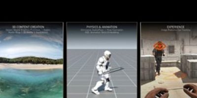
Clock buffers and multiplexers meet PCIe Gen6 specifications

Believed to be the first clock buffers and multiplexers on the market to meet stringent PCIe Gen6 specifications, the RC190xx clock buffers and RC192xx multiplexers have been released by Renesas. 

The release comprises 11 clock buffers and four multiplexers. The devices, which also support and provide extra margin for PCIe Gen5 implementations, complement Renesas’ low-jitter 9SQ440, 9FGV1002 and 9FGV1006 clock generators for PCIe Gen6 timing for data centre / cloud computing, networking and high-speed industrial applications.

The PCIe Gen6 standard supports extremely high data rates of 64Gtransfers per second while requiring very low clock jitter performance of less than 100fs RMS. The RC190xx clock buffers and RC192xx multiplexers have PCIe Gen6 additive jitter specs of only 4fs RMS, making them virtually noiseless, says Renesas. The company claims this means they future-proof designs for the next generation of industry standards.

“PCIe Gen6 timing will be at the heart of new equipment in data centers, high-speed networking and other applications,” said Zaher Baidas, vice president of the Timing Products division at Renesas. 

“It will be interesting to see the innovative implementations that result from this new capability, especially when considering how solutions for the emerging Chiplet market are starting to evolve, with the need for increasing speed and bandwidth as an underlying constant,” comments Rich Wawrzyniak, principal analyst for Semico Research.

The PCIe Gen6 clock buffers and multiplexers offer 1.4ns in-out delay, 35ps out-out skew and -80dB PSRR (power supply rejection ratio) at 100kHz in addition to low 4fs PCIe Gen6 additive jitter. 

Selectable SMBus addresses facilitate the use of multiple devices while SMBus write-protect feature enhances system security. 

The devices represent 30 per cent space-saving compared to earlier devices, adds Renesas.

Other features are loss-of-signal (LOS) output supports system monitoring and redundancy, a four-wire side-band interface to support high speed serial output enable / disable and device daisy-chaining. In addition, power down tolerant (PDT) and flexible start-up sequencing (FSS) features ensure good behaviour under abnormal system conditions, the company claims.

The RC190xx buffers are offered in 4-, 8-, 13-, 16-, 20- and 24-output configurations. The RC192xx multiplexers include 2-, 4-, 8- and 16-output versions. They are offered in packages as small as 3.0 x 3.0mm. 

All of the new devices are available now, and Renesas also offers an evaluation board schematic. 

http://www.renesas.com

> Read More

Wideband transceiver test reveals RF characteristics of mixed digital devices

To accelerate the design cycle, Keysight Technologies has introduced a digital wideband transceiver test system, which it claims unveils true radio frequency (RF) performance characteristics of mixed-digital RF devices.

Defense radars and satellite communications and 5G employ phased-array antennas (PAA) to meet performance and versatility requirements to millimeter wave frequencies. Digital signals are highly integrated into the RF front-end architecture of modern antennas used in defence radar, satellite communications and 5G. As a result, the antennas need a new measurement methodology for stimulus and response measurements, says Keysight.

Its digital wideband transceiver test comprises a vector network analyser, device measurement software and transceiver analysis software to compare digital and RF signals between device input and output and measures the transmitter and receiver responses independently from other test instrumentation. 

The test system uses Keysight’s N52xxB PNA/PNA-X vector network analyser. This is an integrated, flexible microwave test engine for measuring active devices, such as amplifiers, mixers and frequency converters. It also includes S94601B device measurement eXpert software, a configuration assistant that enables users to set up complex measurements for various types of devices. There is also S94610B digital wideband transceiver analysis software. This test waveform creator and configuration assistant enables users to set up mixed-digital RF devices.

Wideband stimulus waveforms are generated by Keysight’s VXG vector signal generator (M938xB) and the PNA-X device measurement eXpert software enables device characterisation and a control interface. The RF test equipment’s measurement and signal fidelity tests new mixed-digital RF devices, and is claimed to minimising errors to yield highest possible performance characteristics.

According to Dan Dunn, vice president of Keysight’s Aerospace & Defense Government Solutions: “Keysight’s digital wideband transceiver test solution enables true RF performance characterisation, while speeding measurements and data analysis that ultimately accelerate the entire design cycle.”

Keysight says the digital wideband transceiver test solution reduces weeks of in-house measurement and data analysis effort to a few minutes. It can be leveraged to component level, such as ADCs, DACs and transceiver ICs as well as sub-system level such as radar / electronic warfare transmit and receive modules, satellite communications transmitters / receivers. For system level, it addresses whole signal paths of 5G PAAs (phased array antennas) using massive multiple-input, multiple-output (MIMO) technology.

The system maintains high measurement accuracy of GHz bandwidth in mm wave frequencies and adapts to proprietary digital designs.

http://www.keysight.com

> Read More

Automotive USB Type-C Power Solution: 45W, 2MHz Buck-Boost Controller in a 1 Inch Square

USB Type-C is a relatively new, high power USB peripheral standard used in computer and portable electronic devices. The USB Type-C standard has driven changes in the USB power delivery specification, allowing for increased bus voltages (up to 20V) and current delivery capability (up to 5A) from the long-standing 5V USB standard. Connected USB-C devices can recognise each other and negotiate a bus voltage – from the default 5V USB output to several higher preset voltage steps – for faster battery charging and higher power delivery where needed, up to 100W.

The simple, compact buck regulators and linear regulators used in battery chargers that require only USB 5V at 500mA to 2A do not sufficiently cover the full range of Type-C USB power. The increased voltage range, 5V to 20V, of Type-C USB power delivery requires more than just step-down voltage conversion from 9V to 36V (or 60V) automotive batteries, or other charging sources. An adjustable buck-boost converter is needed with the ability to both step-up and step-down the input-to-output voltage.

Additionally, for high power automotive USB chargers, a buck-boost converter should support a 10A or higher peak switch current rating and offer low EMI performance. The ability to set the switching frequency outside the AM radio band and maintain a small solution size are sought-after features. High voltage monolithic converters (with onboard switches) are not capable of sustaining such high peak switch currents without burning up.

The LT8390A is a unique 2MHz, synchronous 4-switch buck-boost controller. At 2MHz switching frequency, it can deliver output voltages between 5V and 15V (up to 45W at 3A) to provide power to a connected USB-C device from a car battery. This high controller switching frequency keeps the solution size small, the bandwidth high, and the EMI outside of the AM radio band. Both spread spectrum frequency modulation and low EMI current-sense architecture help LT8390A applications pass the rigors of the CISPR 25 Class 5 automotive EMI standard.

High Power Density Conversion: Size (and Power), Efficiency, Heat

The design of a voltage regulator system operating in an automotive or portable electronics environment is constrained by the space required for the circuit, as well as the heat it generates during operation. These two factors impose an upper bound of achievable power levels while operating within the given design constraints.

Increasing the switching frequency of a design allows for the use of smaller inductors, which is often the largest footprint component in wide input voltage 4-switch buck-boost voltage regulator designs. The LT8390A’s 2MHz switching frequency capability enables the use of a much smaller inductor size than a 150kHz or 400kHz design. A complete design is shown in Figure 1. Along with a smaller inductor, this solution uses only ceramic output capacitors, eliminating the need for bulky electrolytic capacitors. All the components necessary for this design, including the IC, are contained within a small, 1″ inch square footprint, as shown in Figure 1.

Figure 1. Efficient, low EMI USB Type-C power solution that fits in a 1″ square.

Figure 2 shows a 45W LT8390A solution using AEC qualified components. This design experiences a maximum temperature increase of 65°C from the ambient temperature, as shown in Figure 3. Even with the small solution size, the LT8390A system boasts a peak efficiency of 94% while delivering a 45W output, and deviates in efficiency by less than 10% over the input range for each output voltage created, shown in the graphs in Figure 4.

Figure 2. This LT8390A voltage regulator solution provides up to 3A at selectable 5V, 9V, or 15V low EMI outputs using AEC qualified

MOSFETs, magnetics, and capacitors.

Figure 3. While generating 45W of output power, this small circuit’s greatest temperature rise is only 65°C above ambient temperature.

Low EMI for Automotive Applications

The LT8390A has several unique EMI mitigating features that enable high power conversion with low noise performance, which simplifies its implementation in automotive systems. A notable difference between LT8390A and alternative 4-switch controllers is the placement of the inductor current sensing resistor. Most 4-switch buck-boost controllers tend to use a ground-referred current sensing scheme to obtain switch current information, whereas the LT8390A places its current sense resistor in-line with the inductor. By placing the sensing resistor in-line with the inductor, it is effectively removed from both the buck and boost hot loops, shrinking the loops in size and improving the EMI performance.

Along with the architectural advantage of the inductor sensing resistor placement, the LT8390A has built-in spread spectrum frequency modulation to further reduce EMI generated by the controller. Furthermore, the switching edge rate is controlled on both the buck and boost power switches using only a few discrete components to slow the turn-on of the MOSFETs, ensuring the proper balance of high frequency EMI reduction and temperature rise in the power switches. With these EMI-reducing features, the only filtering needed to meet CISPR 25 compliance is taken care of by small ferrite filters on the input and output rather than large ferrite cases and bulky LC filters. The solution shown in Figure 1 was designed using only AEC-Q100 components.

Seamless Output Voltage Transitions

The LT8390A’s output voltage can be adjusted without shutting down the converter by using logic-level signals to drive MOSFETs that adjust the resistor divider off the output to change the set voltage. A USB PD source controller device with GPIO pins can be used in conjunction with the LT8390A system to facilitate the negotiation process between host and USB-connected device and to set the desired bus voltage.

Figure 5 demonstrates how smoothly the output of the LT8390A system transitions from one output voltage to another. When powered from a 12V input source, each transition to an increased output voltage takes at most 150µs to settle, as measured from the rising edge of the digital control signal. During these changes in the output voltage, the buck-boost controller goes through mode transitions – between buck, boost, and buck-boost operation – depending on the relation of input to output voltages. These mode transitions are performed in a controlled manner, preventing excessive overshoot or sagging of the output voltage.

Figure 4. The LT8390A voltage regulator system remains in the 94% to 84% efficiency range across all output voltages generated when powered from an automotive SLA battery.

Figure 5. The output of the LT8390A system smoothly transitions between 5V, 9V, and 15V outputs while maintaining continuous power deliver to the output.

Expanding Beyond 45 W

To push the output power level beyond 45W requires operating at a lower switching frequency to reduce switching losses, which might otherwise thermally stress the MOSFETs at this power level. As an alternative to the LT8390A, the LT8390 operates between 150kHz and 600kHz with the same feature set as LT8390A – allowing low EMI, high power buck-boost designs. A 400kHz LT8390 system, utilising a larger inductor and output capacitor, easily achieves 100W of output power from an automotive battery input with acceptable temperature rise. Figure 6 illustrates the power capabilities of the LT8390A and LT8390 product line from various battery-powered inputs.

Figure 6. The LT8390A and LT8390 cover a wide range of output power levels for USB power delivery.

Conclusion

The new USB standard for voltage regulators powering connected devices permits higher power transfer by increasing the output voltage range and current delivery that regulators can provide. Portable and automotive battery-powered USB-C charger devices require a wide VIN/VOUT buck-boost regulator to deliver a bus voltage above or below the input voltage. The LT8390A provides up to 45W of output power in a small footprint, made possible by its 2MHz switching frequency. For power levels exceeding 45W, the LT8390 can be used with a slightly larger solution size and lower switching frequency.

By Kyle Lawrence

Kyle Lawrence [kyle.lawrence@analog.com] is an applications engineer at Analog Devices. He is responsible for the design and testing of a variety of dc-to-dc converters, including 4-switch buck-boost voltage regulators and LED drivers targeting low EMI automotive applications. Kyle received his B.S. degree in electrical engineering from the University of California, Santa Cruz in 2014.


> Read More

LoRa Edge goes further to enable satellite networks

Semtech has added multi-band capabilities to its LoRa Edge device-to-cloud geolocation platform. The LoRa Edge LR1120 allows for direct satellite-connected IoT applications in supply chain management and logistics.

“With the launch of multi-band LoRa support, coupled with LoRa Cloud™ services, it has never been easier to expand ubiquitous IoT connectivity and geolocation globally,” says Marc Pégulu, vice president of IoT product marketing for Semtech’s Wireless and Sensing Products group.

Intercontinental logistics companies can leverage highly integrated, low power trackers with enhanced interoperability, via the LoRa Edge LR1120. It offers versatile connectivity for a simpler operation and global mobility across multiple regulatory regions, says Semtech. It presents the possibility to offer a low power and low cost sensor with satellite connectivity for capital intensive applications, such as infrastructure monitoring, agriculture and environmental monitoring that require deployment in remote areas.

The LoRa Edge LR1120 offers multi-band LoRa capability (sub-GHz, 2.4GHz and licensed S-band for satellite). It also offers multi-technology geolocation using GNSS for outdoor and Wi-Fi for indoor, as well as areas where satellite coverage is poor.

The LoRa Cloud geolocation solver transfers the location processing workload from the device to the Cloud, making ‘deploy once’ battery life possible. 

The platform is supported by GPS and BeiDou constellations and includes a hardware crypto engine for increased security. 

According to Christopher Taylor, Director, RF & Wireless with Strategy Analytics, “Adding satellite communication capabilities in the S-band to LoRa can help replace aging SCADA monitoring and opens up new applications and markets, especially in remote regions”.

Semtech’s LoRa device-to-Cloud platform is a long range, low power technology for IoT applications. The company says it enables the rapid development and deployment of  low power, cost efficient and long range IoT networks, gateways, sensors, module products and IoT services worldwide. 

The LoRa technology provides the communication layer for the LoRaWAN standard, which is maintained by the LoRa Alliance, an open IoT alliance for Low Power Wide Area Network (LPWAN) applications that has been used to deploy IoT networks in over 170 countries. 

Semtech is a founding member of the LoRa Alliance. 

Semtech supplies analogue and mixed-signal semiconductors and advanced algorithms for infrastructure, consumer and industrial equipment. 

http://www.semtech.com

> Read More

About Smart Cities

This news story is brought to you by smartcitieselectronics.com, the specialist site dedicated to delivering information about what’s new in the Smart City Electronics industry, with daily news updates, new products and industry news. To stay up-to-date, register to receive our weekly newsletters and keep yourself informed on the latest technology news and new products from around the globe. Simply click this link to register here: Smart Cities Registration