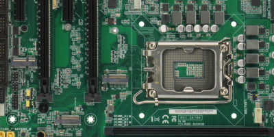
NXP packages automotive radar in single chip 

Claimed to be an industry-first, a family of 28nm RFCMOS radar one-chip ICs has been introduced by NXP for advanced driver assistance systems (ADAS) and autonomous driving systems. 

The SAF85xx family combines NXP’s radar sensing and processing technologies into a single device. They integrate four high-performance transmitters, four receivers, a multi-core radar processor with hardware accelerator, Gigabit Ethernet communication interface and memory into a single device. NXP said, the ICs offer Tier one companies and OEMs flexibility in addressing short, medium and long range radar applications for challenging NCAP safety requirements. 

The SAF85xx family targets the Automotive Safety Integrity Level B (ASIL B) requirements, according to the ISO 26262 functional safety standard and the automotive cybersecurity standard ISO/SAE 21434 to meet the requirements of the automotive industry for safety and security.

The family of automotive radar SoCs is comprised of radar transceivers integrated with multi-core radar processors which are built on NXP’s S32R radar compute platform. The SAF85xx offers twice the RF performance and accelerates radar signal processing by up to 40 per cent, compared to NXP’s previous generation. 

The one-chip family enables 4D sensing for corner and front radar, for ADAS applications such as automated emergency braking, adaptive cruise control, blind-spot monitoring, cross-traffic alert and automated parking.

The single chip radar ICs enable “the reliable long range detection of objects and separation of small objects next to larger ones, like a fast-moving motorcycle next to cars and trucks on a busy multi-lane highway,” said Torsten Lehmann, executive vice president, NXP Semiconductors. “Its small form factor allows our customers to build radar sensor modules that are up to 30 per cent smaller,” he added, which is expected to expand the potential of radar safety.

The SAF85xx one-chip family is sampling now for alpha customers. 

http://www.nxp.com

> Read More

Optical gyroscope with GNSS/INS evaluation kit tracks autonomous vehicles

Tracking technology developed by Anello uses an on-chip waveguide manufacturing process, integrated with a patented silicon photonic IC to enable fibre optic gyro performance with a standard silicon manufacturing process.

The SIPHOG (Silicon Photonics Optical Gyroscope) is intended for the autonomous navigation market and Anello’s evaluation kit is expected to be used for mapping, surveying, robotics, construction, defence, aerospace and autonomous vehicle applications.

The SIPHOG’s principle of operation is the same as that of the classical interferometric fibre optic gyroscope where the phased modulated light is launched into a waveguide where the light experiences equal but opposite additional phase shifts during rotation. This additional phase shift, due to rotation, is known as the Sagnac effect. The return light from the waveguide is coupled into a photodetector, where the two return beams produce an interference signal that is linearly proportional to the angular rate.

Anello’s low loss on chip waveguide manufacturing process allows the “fibre” in a FOG to be directly replaced by the patented SIPHOG waveguide IC. The IC replaces the discrete optical components (couplers, modulators and detector) found in a FOG. The integrated SIPHOG therefore reduces component costs and dimensional volume compared to an equivalent high performance traditional fibre optic gyro (FOG) implementation.

 The manufacturing process is being developed at a large USA-based commercial semiconductor foundry.

Powered by Anello’s optical gyroscope and sensor fusion engine, the evaluation kit can maintain centimetre accuracy in conditions where more expensive ground-truth positioning and localisation systems degrade, said the company. The kit is also accurate in extended full GNSS loss operation. Unlike other positioning and localisation systems, the evaluation kit is more stable over wide temperature ranges and under extreme vibration, said Anello.

The kit has been designed to be easy to use while enabling seamless navigation and positioning in challenging GNSS-denied environments where accuracy is paramount.

Anello reported that it is currently engaged in trials with customers in the automotive, robotics, autonomy, construction, heavy vehicles, defence, aerospace, mapping and surveying markets.

Anello Photonics is based in Santa Clara, California, USA. It has developed an integrated photonic SoC technology for next generation navigation. Its SiPhOG gyroscope is based on its proprietary waveguide process that mimics the properties of optical fibre in an on-chip waveguide. 

http://www.anellophotonics.com

> Read More

Smart lock and energy harvesting secure wireless power

Infineon Technologies has announced that wireless power system company, NuCurrent, is an Infineon Preferred Partner. The partnership launches with a focus on Infineon’s energy harvesting actuator and sensing ICs. With NuCurrent and Infineon technology, devices will implement optimised, contactless access and entry, eliminating or minimising the need for batteries in many applications. 

NuCurrent’s design tools enable IP and development services which allow OEMs a faster route-to-market.

Infineon’s NFC tag-side controllers with integrated H-bridge and energy harvesting modules are a single-chip solution for developing cost-effective, miniaturised actuation or sensing applications operating in passive or active mode. The partnership will incorporate NuCurrent’s wireless power systems technology and design capabilities.

“NFC wireless energy harvesting and charging are game-changing technologies from various perspectives: product design, environmental sustainability, and user experience,” said Jacob Babcock, CEO of NuCurrent. As the capabilities of energy harvesting expand NFC is expected to deliver new features to product developers.

“Infineon and NuCurrent are bringing together complementary capabilities that are paving the way for new solutions eliminating batteries in locks, sensors, and other applications via contactless energy transfer,” explained Doris Keitel-Schulz, vice president of Contactless Power and Sensing at Infineon. “We are providing a reliable, low-maintenance, and secure replacement to batteries that significantly reduces e-waste. Our energy harvesting technology via mobile phone NFC field enables the digitalisation of the passive world and connects them into the mobile phone ecosystem,” she said.

Over time, the partnership is expected to produce solutions for varied applications, particularly locks in industrial, office, and hospital settings. 

For sensor applications, the partnership enables new categories of applications where sensors do not require batteries and are triggered by NFC energy harvesting. An example of potential applications is a smart lock with energy harvesting features, showcased at CES 2023 in Las Vegas.

NuCurrent supplies wireless power technologies and product integration, spanning  span magnetics, software and systems simulation. The company holds over 300 patents and systems integration expertise which supports manufacturers of appliances, smartphones, wearables, hearables, consumer electronics, medical devices, robotics, IoT, sporting equipment and other emerging product categories.

http://www.nucurrent.com

http://www.infineon.com

> Read More

Marktech Optoelectronics introduces two InGaAs photodiode photodetectors

Optoelectronics designer and manufacturer, Marktech Optoelectronics has released  two indium gallium arsenide (InGaAs) photodiode photodetectors with extended 2.6 micron wavelength responsivity cut offs.

The high speed 2.6 micron InGaAs PIN photodiodes have sensitivity wavelength ranges of 600 to 2,600nm with active area diameters of 1.0mm.

The MTPD2601T-100 InGaAs photodiode is packaged in a TO-46 hermetic metal can with a flat lens and the MTPD2601N-100 InGaAs component uses a TO-46 package with a domed lens. TO metal can packaging provides the highest protection against the ingress of vapour and moisture, said the company, which contributes to reliable, long lifetime InGaAs photodiode detectors.

The 2.6 micron InGaAs photodiode detectors in a TO metal can packages are available now through distributors Digikey Electronics and Mouser Electronics.

Marktech’s InGaAs photodiode manufacturing partner in Japan, Optrans, is recognised as producing some of the industry’s highest integrity visible through SWIR (short wave infra red) detectors.  

In addition to standard InGaAs detectors, Marktech can provide many additional services often required to rapidly move a project from the design to the finished product stage, such as detector and emitter selection, application and specification development, InGaAs photodiode customisation, package type selection and custom packages,electro-optical testing and troubleshooting, circuit and assembly design and build and supply of InGaAs photodiodes.

Standard offerings are 1.7 and 2.6 micron but Optrans can tailor the peak responsivity to wavelengths lower than 2.6 micron for applications with sufficiently high annual volumes. 

InGaAs PIN photodiodes are available in various package types such as hermetically sealed metal cans (TO-5, TO-18, and TO-39), ceramic SAW packages, pigtail cans, 3mm molded plastic through-hole (flat lens or dome ceramic), and Marktech’s latest enhanced SMD packaging system, the hermetic Atlas package. 

Custom-engineered packaging to OEM specifications are also available.

The high sensitivity of InGaAs detectors combined with low noise characteristics (high signal/noise ratio) in the NIR and SWIR wavelengths make InGaAs suitable for medical devices and wearables such as glucose monitoring (non-contact, optical), blood alcohol monitoring, exhaled breath gas analysis, urinalysis. In the field of spectrometry, they can be used for FTIR spectrometry, Raman spectroscopy, tunable diode laser spectroscopy (TDLS), scanning or dispersive NIR spectrometry, non-dispersive infra red (NDIR) spectroscopy, electroluminescence and fluorescence spectrometry, emerging infra red spectroscopy methods, temperature and flame detection, infra red pyrometry or non-contact radiation thermometers, flame and spark detection and regulation, moisture detection and compositional sorting, moisture meters (spectrophotometric), precision agriculture, food sorting and food quality instruments, plastics sorting and recycling. 

For photonics test instrumentation, they can be used for coherent measurement systems, IR laser diode characterisation and monitoring, monitoring SWIR LEDs and illuminators, optical power meters, communication receivers in the O, L, and C bands, gas sensing, optical coherence tomography (OCT) and lidar.

Marktech also has capabilities to design and manufacture custom photodetectors to OEM specifications from prototype to production volumes. These include custom photodetector engineering and the manufacturing range includes custom InGaAs photodiodes (wafers, die, packaged InGaAs PDs, and assemblies). In addition, Marktech can co-package InGaAs photodiodes with emitters, filters, thermoelectric coolers (TECs), and transimpedance amplifiers (TIAs). 

InGaAs photodiodes from Optrans Japan and silicon photodiodes from Marktech’s Simi Valley plant are assembled in the same package to produce wide spectral band detectors – (SWIR/MIR to mid UVB). This technology makes hybrid InGaAs-silicon detectors with responsivities from 250 to 2,600nm feasible.

https://www.marktechopto.com

> Read More

About Smart Cities

This news story is brought to you by smartcitieselectronics.com, the specialist site dedicated to delivering information about what’s new in the Smart City Electronics industry, with daily news updates, new products and industry news. To stay up-to-date, register to receive our weekly newsletters and keep yourself informed on the latest technology news and new products from around the globe. Simply click this link to register here: Smart Cities Registration