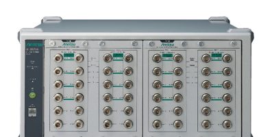
Magnachip introduces 600V SJ MOSFETs with fast recovery body diodes

Magnachip has introduced 600V super junction MOSFETs with RDS(on) as low as 44 mOhm for EV chargers and servers. There are nine products in the 600V MOSFET family, featuring the proprietary design technology.

Magnachip’s design provides specific on-resistance (RSP) reduction of about 10 per cent, achieved while maintaining the same cell-pitches of previous generation MOSFETs.

The 600V super junction MOSFETs are equipped with a fast recovery body diode. The proprietary technology significantly enhances system efficiency with reduced reverse recovery time (trr) and switching loss. Therefore, the figure of merit to evaluate general performance of MOSFETs was improved by more than 10 per cent compared to the previous generation, said Magnachip. The 600V super junction MOSFETs can be used widely in industrial applications, such as solar inverters, energy storage systems, uninterruptible power supply systems, and a variety of electronics.

One of the nine MOSFETs is the MMQ60R044RFTH which offers a low RDS(on) of 44 mOhm, making it suitable for electric vehicle chargers and servers. 

“Now that we have introduced these 600V SJ MOSFET products, we are aiming to unveil new 650V and 700V SJ MOSFET products with fast recovery body diode in the second half of 2023,” said YJ Kim, CEO of Magnachip. 

Magnachip Semiconductor is a designer and manufacturer of analogue and mixed-signal semiconductor platforms for communications, IoT, consumer, computing, industrial and automotive applications. The company has more than 40 years’ of operating history, owns a portfolio of approximately 1,100 registered patents and pending applications, and has extensive engineering, design and manufacturing process expertise. 

http://www.magnachip.com

> Read More

Axelera IP uses Arteris IP to accelerate edge computer vision 

The Metis AI platform for AI at the edge is based on Arteris FlexWay IP. The network on chip system IP allows engineers to meet performance and power objectives while reducing time to market, said Arteris.

Arteris FlexWay IP will be used for SoC connectivity in the Metis AI platform, which is a hardware and software platform for computer vision AI inference at the edge.

The Metis AI processing unit (AIPU), as part of the Metris AI Platform, is equipped with four homogeneous AI cores built for complete neural network inference acceleration. Each AI core is self-sufficient and can execute all layers of a standard neural network without external interactions. The four cores are integrated into an SoC and comprised of a RISC-V controller, PCIe interface, LPDDR4X controller, and a security complex connected via a high speed network on chip (NoC). The unit can collaborate on a workload to boost throughput or operate on the same neural network in parallel to reduce latency. It can also process different neural networks required by the application concurrently.

Giuseppe Garcea, director of silicon and co-founder at Axelera AI, said: “Arteris FlexWay interconnect IP allowed us to close timing smoothly on a complex, multicore machine learning architecture”.

Arteris FlexWay interconnect IP uses area-optimised interconnect components to address a smaller class of SoC. The architecture has been designed to be compatible with Arm AMBA AXI and AHB standards. It provides a scalable solution to ultra-low power consumption and the automation of interconnect SoC connectivity.

Arteris provides system IP for the acceleration of SoC development across electronic systems. Arteris network on chip (NoC) interconnect IP and IP deployment technology enable higher product performance with lower power consumption and faster time to market, delivering better SoC economics.

Axelera AI designs AI at the edge. Its Metis AI platform is a holistic hardware and software solution for AI inference at the edge. It enables computer vision applications to become more accessible, powerful and user-friendly, claims the company. 

Headquartered in the AI Innovation Center of the High Tech Campus in Eindhoven, Axelera AI has R&D offices in Belgium, Switzerland, Italy and the UK. Its team of experts in AI software and hardware hail from top AI firms and Fortune 500 companies. 

The Metis AI platform is available for pre-ordering at the Axelera AI website and a select group of customers via the Early Access Program.  

https://www.arteris.com 

> Read More

Design flows are based on the Integrity 3D-IC platform 

Design flows based on the Integrity 3D-IC platform have been announced by Cadence Design Systems to support the TSMC 3Dblox standard for 3D front end design partitioning in complex systems. 

Cadence flows are optimised for all of TSMC’s latest 3DFabric offerings, including integrated fan-out (InFO), Chip-on-Wafer-on-Substrate (CoWoS) and System-on-Integrated-Chips (TSMC-SoIC) technologies. By using these design flows, customers can accelerate the development of advanced multi-die package designs for emerging 5G, AI, mobile, hyperscale computing and IoT applications, said Cadence.

The Cadence Integrity 3D-IC platform combines system planning, packaging, and system level analysis and is certified for use with the TSMC 3DFabric and the 3Dblox 1.5 specification. The flows based on this platform incorporate new features like 3D routability-driven bump assignment and hierarchical bump resource planning. 3Dblox, which is inherently supported by the Integrity 3D-IC platform, provides a seamless interface for Cadence system analysis tools for early power delivery network (PDN) and thermal analysis via the Cadence Voltus IC Power Integrity Solution and Celsius Thermal Solver system analysis tools; extraction and static timing analysis via the Cadence Quantus Extraction Solution and Tempus Timing Signoff and system level layout versus schematic (LVS) checks via the Cadence Pegasus Verification system.

“3D-IC technology is key to meeting the performance, physical size, and power consumption requirements to enable next-generation HPC and mobile applications,” said Dan Kochpatcharin, head of the design infrastructure management division at TSMC. “By continuing our collaboration with Cadence, we’re enabling customers to leverage our comprehensive 3DFabric technologies and the Cadence flows that support our 3Dblox standard, so they can significantly improve 3D-IC design productivity and speed time to market,” he added.

“The Cadence flows based on the Integrity 3D-IC platform incorporate everything a customer needs to quickly design a leading-edge 3D-IC using TSMC’s latest 3DFabric technologies,” added Dr. Chin-Chi Teng, senior vice president and general manager in the digital and signoff group at Cadence.

The Cadence Integrity 3D-IC platform, including Allegro X packaging technologies, is part of the company’s broader 3D-IC offering and aligns with the Cadence Intelligent System Design™ strategy, enabling SoC design excellence. The Cadence reference flows and tutorials are available on TSMC Online now.

http://www.cadence.com

> Read More

Simplicity Studio supports Mikroe’s mikroSDK 2.0 Click board driver

Silicon Labs is the first IC vendor to integrate MikroElektronika (Mikroe)’s mikroSDK Click Board drivers to its software environment. 

Support for the mikroSDK 2.0 Click drivers was achieved by adding a hardware driver extension (plugin) into Mikroe’s Gecko SDK (software development kit), which is now available within Silicon Labs’ Simplicity Studio IDE (integrated development environment). This integration means embedded engineers can use the Mikroe peripheral Click boards to develop both the hardware and software for an embedded system based on Silicon Labs’ controllers.

Nebojsa Matic, Mikroe’s CEO, said: “Many IC vendors now include the mikroBUS socket standard on their development boards. This enables developers to try out thousands of different peripheral Click boards, saving hardware cost and design time”. The addition of the mikroBUS socket in Silicon Labs’ Explorer Kits, has added hardware driver extension support for the mikroSDK 2.0 Click drivers into the silicon company’s IDE, Simplicity Studio GSDK which will allow designers using Silicon Labs SoCs or microcontrollers to easily include Click board libraries into their code. According to Matic, this means that engineers will save time and money by using the Click boards hardware, but they will have also seamlessly addressed the software task too. “It’s a real validation of our approach,” he added.

Anders Pettesson, director of mass market marketing at Silicon Labs, added: “After partnering with Mikroe on Click board projects and seeing the possibilities of the ecosystem, we decided to bring that flexibility and ease of use to the Silicon Labs environment. By creating the mikroSDK 2.0 Click driver extension, we’ve now made it easy for embedded engineers to add thousands of peripherals to Silicon Labs software projects.” 

MikroElektronika (Mikroe) invented the mikroBUS development socket standard and the compact Click boards for peripherals that use the standard to dramatically cut development time. Since its introduction in 2011, the company now offers 1350+ Click boards – 10 times more than competitors. The mikroBUS standard is included by leading microcontroller companies on their development boards. 

SiBrain is Mikroe’s standard for microcontroller development add-on boards and sockets and the company’s DISCON  standard enables uses to choose between a wide variety of supported LCDs and touchscreen options. Mikroe also offers the NECTO IDE and a wide range of compilers, development boards, programmers and debuggers.

http://www.mikroe.com

> Read More

About Smart Cities

This news story is brought to you by smartcitieselectronics.com, the specialist site dedicated to delivering information about what’s new in the Smart City Electronics industry, with daily news updates, new products and industry news. To stay up-to-date, register to receive our weekly newsletters and keep yourself informed on the latest technology news and new products from around the globe. Simply click this link to register here: Smart Cities Registration