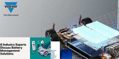
Multi-mode cellular and satellite IoT module has embedded positioning 

Developed to ensure seamless connectivity even when no terrestrial cellular network is available, the u-blox SARA-S520M10L is the company’s cellular and satellite IoT module with accurate, low power positioning and “ubiquitous connectivity” said u-blox. 

The module’s communication and tracking capability makes it suitable for asset tracking, fleet management, maritime transportation, mining, utilities and smart agriculture applications. It also serves market segments such as anti-theft systems, industrial monitoring and control, and applications that require communication in safety-critical scenarios, advised u-blox. 

At approximately 400mm2, the u-blox SARA-S520M10L is claimed to be the smallest multi-mode cellular and satellite IoT module on the market. It provides LTE-M/NB-IoT, L-band satellite connectivity, and embedded navigation capability for connectivity through terrestrial cellular networks and geostationary (GEO) satellites. It can provide location fixes using up to four satellite constellations and is pin-compatible with other u-blox cellular-only modules in the SARA form factor.  

This is the first u-blox module designed with the 2nd generation of the u-blox UBX-R5 chip, the UBX-R52/S52. The S52 variant was developed to support satellite IoT communication alongside LTE-M/NB-IoT cellular standards. 

“Comparable solutions on the market require two distinct subsystems, one for cellular and another for satellite connectivity,” said Alessandro Bonetti, senior product manager, product centre cellular at u-blox. Building the module around a single, highly integrated, multi-mode modem SoC reduces size and complexity, Bonetti added. He said the versatile SoC, combined with the company’s GNSS capability serves mobile and stationary IoT applications in “challenging environments such as isolated places, mountains, or in the middle of the ocean”. 

The first samples will be available by Q1 2024.

u-blox specialises in positioning and wireless communication in automotive, industrial and consumer markets. The company’s services, and products let people, vehicles, and machines determine their precise position and communicate wirelessly over cellular and short range networks. It offers a broad portfolio of chips, modules, and secure data services and connectivity to develop solutions for the IoT quickly and cost-effectively. With headquarters in Thalwil, Switzerland, the company has offices in Europe, Asia, and the USA. 

http://www.u-blox.com

> Read More

MRigidCSP package is claimed to increase MOSFET’s mechanical strength  

Robust package technology, MRigidCSP, by Alpha and Omega Semiconductor (AOS), is initially offered on its AOCR33105E, 12V, common drain, dual N-channel MOSFET. The packaging technology is designed to decrease on resistance while increasing mechanical strength, and is particularly suited to battery applications in smartphones, tablets and ultra-thin notebooks.
AOS explained that fast charging, which requires lower power loss in the battery management circuit, is now widely adopted for portable devices. As the charging currents increase, ultra-low electrical resistance is needed for improved performance. In standard wafer-level chip scale packages (WL-CSPs), the substrate can be a significant portion of the total resistance when back-to-back MOSFETs are employed in battery management applications.  A thinner substrate reduces the overall resistance but drastically reduces the package’s mechanical strength. This reduction of mechanical strength can lead to more stress during the PCB assembly reflow process, potentially causing warping or cracking in the die and, ultimately, failure in the application. The AOCR33105E is designed with trench-power MOSFET technology in a common drain configuration for design simplicity. It features low on resistance with ESD protection to improve performance and safety in battery management, such as protection switches and mobile battery charging and discharging circuits.
“Incorporating the AOS MRigidCSP packaging technology with our new dual N-channel MOSFET combines electrical performance improvements with the benefit of high robustness,” said Peter H. Wilson, senior MOSFET product line marketing director at AOS.
AOS designed the MRigidCSP package technology to be used with high aspect ratio CSP die sizes. The CSP construction delivers “a significantly strengthened battery MOSFET that won’t warp or break during the board manufacturing process,” added Wilson.
The AOCR33105E is available in a 2.08 x 1.45mm package, with RDS(on) of 3mOhm at 4.5V / 4.2mOhm at 3.1V.
The AOCR33105E in the MRigidCSP package is immediately available in production quantities with a lead time of 14 to 16 weeks. It is RoHS 2.0 compliant and is halogen-free.

http://www.aosmd.com

> Read More

Ultrasonic ToF sensor have high computational power

Available in a reflowable package, the SmartSonic ICU-20201 ultrasonic ToF (time of flight) sensor has been designed by TDK in a miniature 3.5 x 3.5mm2 form factor.

It integrates a PMUT (piezoelectric micromachined ultrasonic transducer) with an low power SoC in the miniature package. Based on ultrasonic pulse-echo measurements, the ToF sensor provides millimeter-accurate and robust range measurements to targets at distances up to 5m over a wide and configurable field of view on any surface and under any lighting condition, said TDK. The company added that these results are possible in any lighting condition, including full sunlight, and independently of the target’s colour and optical transparency.

It also has a powerful embedded processor and extended memory space for high computational power, sufficient to allow complete application algorithms directly on the chip.

Typical applications are sensing accuracy in robotics, drones, smart homes or buildings and mobile devices. It can also be used in enterprise settings that require shelf inventory monitoring or level sensing, such as in smart homes or smart buildings.

Massimo Mascotto is director of product marketing at InvenSense, a TDK Group company. He said that the ICU-20201’s “increased computational capability enables smarter product design and an enhanced end user experience”.

The ICU-20201 is available now.

TDK was established in 1935 to commercialise ferrite, a key material in electronic and magnetic products. TDK‘s portfolio features passive components such as ceramic, aluminium electrolytic and film capacitors, as well as magnetics, high-frequency and piezo and protection devices. The company also provides sensors and sensor systems such as temperature and pressure, magnetic and MEMS sensors. In addition, TDK provides power supplies and energy devices and magnetic heads. These products are marketed under the product brands TDK, Epcos, InvenSense, Micronas, Tronics and TDK-Lambda. 

TDK focuses on demanding markets in automotive, industrial and consumer electronics, and information and communication technology. The company has a network of design and manufacturing locations and sales offices in Asia, Europe, and in North and South America. 

InvenSense is a TDK Group company and targets the consumer electronics and industrial areas with integrated motion, sound, pressure and ultrasonic solutions. InvenSense’s productss combine MEMS (micro electrical mechanical systems) sensors, such as accelerometers, gyroscopes, compasses, microphones, barometric pressure sensors, and ultrasonic time-of-flight sensors with proprietary algorithms and firmware that intelligently process, synthesise, and calibrate the output of sensors, maximising performance and accuracy. InvenSense’s motion tracking, ultrasonic, audio, fingerprint, location platforms and services can be found in mobile, wearables, smart home, industrial, automotive, IoT and robotics.

InvenSense became part of the MEMS sensors business group within the Sensor systems business of TDK in 2017. In April of 2022, Chirp Microsystems formally merged with InvenSense. InvenSense is headquartered in San Jose, California, USA and has offices worldwide.

https://invensense.tdk.com/

> Read More

Cadence-Arm collaboration pushes Neoverse V2 verification

Cadence Design Systems has collaborated with Arm for its Neoverse V2 by fine-tuning its AI-driven RTL-to-GDS digital flow for Neoverse V2 and delivered corresponding 5nm and 3nm Rapid Adoption Kits (RAKs) which are designed to support customers achieve power, performance and area (PPA) targets faster. The Cadence AI-driven verification full flow supports Neoverse V2, providing designers with optimal verification throughput and preparedness for Arm SystemReady compliance, added Cadence.
The AI-driven Cadence RTL-to-GDS digital full flow RAKs for 3nm and 5nm nodes include Genus Synthesis, Modus DFT Software, Innovus Implementation System, Quantus Extraction, Tempus Timing and ECO Option, Voltus IC Power Integrity, Conformal Equivalence Checking, Conformal Low Power and the AI-based Cerebrus Intelligent Chip Explorer.
Benefits of the digital RAKs for Arm Neoverse V2 designers include, for example, the  Cerebrus AI capabilities which automate and scale digital chip design, delivering better PPA and improving designer productivity. The inclusion of Cadence iSpatial technology provides an integrated and predictable implementation flow for the faster design closure, added the company. The RAKs also include a smart hierarchy flow that delivers optimal turnaround times on large, high-performance CPUs.
In another example, the Tempus ECO technology offers sign off-accurate final design closure based on path-based analysis. The incorporation of the GigaOpt activity-aware power optimisation engine is claimed to significantly reduce dynamic power consumption.
The AI-driven verification full flow is optimised to support Arm Neoverse V2 and includes the Xcelium Logic Simulation platform, Palladium Enterprise Emulation platforms, Protium Enterprise Prototyping systems, Helium Virtual and Hybrid Studio, Jasper Formal Verification platform, Verisium Manager Planning and Coverage Closure tools, Perspec System Verifier, and VIP and System VIP tools and content for Arm-based designs.
The verification full flow provides Neoverse V2 designers with pre-silicon server base system architecture (SBSA) compliance verification and optimised PCI Express (PCIe) integration while the Helium Virtual and Hybrid Studio includes editable virtual and hybrid platform reference designs for Neoverse V2. These designs incorporate Arm Fast Models to jumpstart early software development and verification. The Helium gearshift technology enables customers to position workloads in a high-performance hybrid environment before shifting to a fully accurate RTL environment, offering detailed verification using either the Palladium or Protium platforms.
“The growing demand for complex workloads such as big data analytics, HPC and ML inference requires specialised compute solutions that achieve greater performance and efficiency,” said Eddie Ramirez, vice president of go-to-market, infrastructure line of business at Arm. “Through this latest collaboration, customers can leverage Cadence’s comprehensive digital and verification flows to validate their solutions and bring the power of their Neoverse V2-based products to market faster. Furthermore, silicon partners will get the benefits of these advanced design flows when running their EDA workloads on Arm-enabled servers and cloud instances.”

http://www.cadence.com

> Read More

About Smart Cities

This news story is brought to you by smartcitieselectronics.com, the specialist site dedicated to delivering information about what’s new in the Smart City Electronics industry, with daily news updates, new products and industry news. To stay up-to-date, register to receive our weekly newsletters and keep yourself informed on the latest technology news and new products from around the globe. Simply click this link to register here: Smart Cities Registration