TDK has announced an expansion to the TDK-Lambda i7A series of non-isolated buck (step-down) DC-DC converters with the industry-standard 1/16th brick pinout. 20A output models with a 500W maximum rating are now available, offering a trimmable 3.3 – 32V* output capability and operation from 28V up to 60V input. An adjustable over-current limit is also available as an option, reducing stress on the converter or load when exposed to excessive overcurrent conditions and facilitating fine-tuning based on actual system requirements.
The 20A i7A models can be used to derive additional high-power outputs at a lower cost and higher efficiency than isolated DC-DC converters. These very compact products are suited for use in mobile robotics, drones, medical, industrial, test and measurement, communications, computing, and portable battery-powered equipment.
Efficiencies of up to 96% dramatically minimise internal losses and allow the 20A i7A models to operate in ambient temperatures of -40°C up to +125°C, even with low airflow conditions. The i7A’s design provides low output ripple and excellent response to dynamic loads. Minimal external components are required, compared to discrete solutions, saving cost and printed circuit board space.
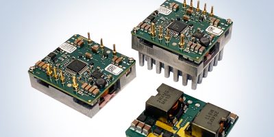
Like the i7A 33A, 45A and 60A versions, the 20A offers a choice of three mechanical configurations, measuring just 34mm wide and 36.8mm in length. The 11.5mm high open-frame model is suitable for applications requiring a low profile and weighs just 25g. The baseplate version can be conduction-cooled to a cold plate and is 12.7mm high. Models with an integral heatsink, which are for convection or forced air cooling, are 24.9mm high.
The i7A standard features include output voltage adjustment, positive remote sense, negative logic remote on-off, input under-voltage, over-current and over-temperature protection. Evaluation boards are available for simplified qualification.
All models have safety certification to the IEC/UL/CSA/EN 62368-1 standards, with CE and UKCA marking to the Low Voltage and RoHS Directives.