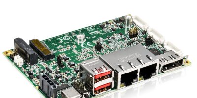
R&S verifies NXP’s next generation automotive radar sensor reference design for extremely short object distances

The radar target simulator R&S RTS has been used to verify the performance of NXP® Semiconductors’ next-generation radar sensor reference design. This collaboration enables the automotive industry to take another step forward in the development of automotive radar, the principal technology that enables advanced driver assistance systems (ADAS) and autonomous driving features.

Engineers from both companies conducted a comprehensive series of tests to verify the new sensor reference design which is based on a NXP’s 28 nm RFCMOS radar one-chip SoC (SAF85xx). The R&S RTS radar test system combines the R&S AREG800 automotive radar echo generator with the R&S QAT100 antenna mmW frontend, offering unique short-distance object simulation capabilities as well as superior RF performance and advanced signal processing with many advanced functions. This enables realistic tests of next generation automotive radar applications and brings automotive industry’s vision of fully autonomous driving one step closer.

NXP’s next generation automotive radar sensor reference design is enabled by the industry’s first 28 nm RFCMOS radar one-chip SoC family leveraging the R&S RTS radar test system. The radar sensor reference design can be used for short, medium and long-range radar applications to serve challenging NCAP (NCAP: New Car Assessment Program) safety requirements as well as comfort functions like highway pilot or urban pilot for the fast-growing segment of L2+ and L3 vehicles.

The R&S RTS is the only test system suitable for complete characterisation of radar sensors and radar echo generation with object distances down to the airgap value of the radar under test. It combines the R&S AREG800A automotive radar echo generator as a backend and the R&S QAT100 antenna array or the R&S AREG8-81S as a frontend. The technically superior test solution is suitable for the whole automotive radar lifecycle including development lab, hardware-in-the-loop (HIL), vehicle-in-the-loop (VIL), validation and production application requirements. The solution is also fully scalable and can emulate the most complex traffic scenarios for advanced driver assistance systems.

Adi Baumann, Senior Director ADAS R&D, at NXP Semiconductors says: “We have been collaborating closely and successfully with Rohde & Schwarz for many years on the verification of our automotive radar sensor reference designs. Rohde & Schwarz’ cutting-edge automotive radar test systems allows us high-quality and highly efficient validation of our automotive radar products and proves outstanding performance of our radar one-chip. The level of experience, quality and support that Rohde & Schwarz provides to NXP is making a difference.”

Gerald Tietscher, Vice President Signal Generators, Power Supplies and Meters from Rohde & Schwarz says: “We are grateful for the collaboration with NXP to accelerate the deployment of advanced automotive radar sensors based on 28 nm automotive radar chips. They serve ever more challenging NCAP safety requirements and will help enable new safety applications. Our experience in automotive radar testing allows us to provide a best-in-class test solution for this radar sensor design based on the industry’s first 28 nm RFCMOS one-chip radar SoC.”

NXP will present the latest developments for radar including the automotive radar sensor reference design at CES 2024 trade show in Las Vegas from January 9 to 12, 2024, at booth CP18.

https://www.rohde-schwarz.com/

> Read More

New, robust approach to overvoltage protection for sensitive electronic signal inputs

High demands on the robustness of electronic systems, especially in industrial environments, continually present developers with great challenges. Overvoltage protection is one key design consideration and challenge, as additional components are usually required to protect systems from overvoltage events – yet they frequently impact and, in the worst case, can even falsify signals. Beyond that, these components incur additional costs and contribute to spatial constraints. Hence, when designing the protection circuit, traditional solutions often require a compromise between system accuracy and the protection level.

Typically, a common and simple design method uses external protection diodes, usually transient voltage suppressor (TVS) diodes, clamped between the signal line and supply or ground. TVS diodes are advantageous as they can react instantaneously to temporary voltage spikes. This type of external overvoltage protection is shown on the left side of Figure 1.

Figure 1. Traditional overvoltage protection design with additional discrete components.
If a positive transient voltage pulse occurs, it is clamped with a current through diode D1 to VDD. The voltage is thereby limited to VDD plus the diode forward voltage. If the pulse is negative and less than VSS, the same applies with the exception that it is clamped to VSS via D2. However, if the leakage current caused by the overvoltage is not limited, it may damage the diodes. For this reason, there is also a current-limiting resistor in the path. For very harsh environmental conditions, an input-side bidirectional TVS diode is often used for enhanced protection.
The disadvantages resulting from this type of protection circuit appear – for example, in the form of increased edge rise and fall times and capacitive effects. Moreover, it doesn’t provide any protection when the circuit is in the de-energised state.
The actual components, such as analogue-to-digital converters (ADCs), operational amplifiers, etc., usually have integrated protection. This can consist of a switch architecture, as shown on the right side of Figure 1. Figure 1 also shows that input-side and output-side protection diodes are present on both supply rails. The downside to this setup is that, when floating signals appear in a de-energized state (the IC is not powered up), the switch may act as if it is active (even if it is set to OFF) as current will flow through the diodes and the power supply rails. This allows current to pass through, resulting in the signal line losing its protection.

Fault-Protected Switch Architecture
One solution to the challenges mentioned above is a fault-protected switch architecture supplemented by a bidirectional ESD cell, as can be seen in Figure 2. Instead of the input-side TVS diodes, now the ESD cell clamps voltage transients by constantly comparing the input voltage with VDD or VSS. In the case of permanent overvoltage, the downstream switch opens automatically. The input voltage is no longer limited by the protection diodes clamped to the supply rails. The limiting factor is now the maximum voltage rating of the switch. Higher system robustness and reliability are additional advantages. There is also virtually no effect on the actual signals and their accuracy. Moreover, the additional current-limiting resistor is not needed because the leakage currents are very low when the switch is open.

Figure 2. Overvoltage protection with integrated bidirectional ESD cell.

This type of input structure is characteristic of the quad SPST (single-pole, single-throw) switch ADG5412F from Analog Devices Inc. (ADI). This switch permits a permanent overvoltage of up to ±55V, regardless of any existing voltage supply. The ESD cell integrated on each of the four channels clamps voltage transients of up to 5.5kV. In an overvoltage condition, only the affected channel is opened and the other channels continue operating normally.

Conclusion
Thanks to this type of overvoltage protection switches, electrical circuits can be greatly simplified. The advantages over the conventional discrete solution are multitudinous, both in terms of guaranteeing optimal switching performance and robustness in a precise signal chain and in terms of spatial optimisation. Hence, the overvoltage protection offered by the ADG5412F is especially suitable for high precision measurement applications in harsh environments.

About the Author
Thomas Brand began his career at Analog Devices in Munich in 2015 as part of his master’s thesis. After graduating, he was part of a trainee program at Analog Devices. In 2017, he became a field applications engineer. Thomas supports large industrial customers in Central Europe and also specialises in the field of Industrial Ethernet. He studied electrical engineering at the University of Cooperative Education in Mosbach before completing his postgraduate studies in international sales with a master’s degree at the University of Applied Sciences in Constance. He can be reached at thomas.brand@analog.com.


> Read More

SemiQ unveils high-performance QSiC power modules in half-bridge packages

SemiQ has expanded its QSiC power modules portfolio with the introduction of a new series of 1200V silicon-carbide (SiC) power MOSFETs in half-bridge packages.

Engineered and tested to operate reliably in demanding environments, these new compact, high-performance modules enable high-power-density implementations while minimising dynamic and static losses. Featuring high breakdown voltage (>1400V), the new QSiC modules support high-temperature operation (Tj = 175°C) with low Rds(On) shift over the full temperature range. In addition, the modules exhibit industry-leading gate oxide stability and long gate oxide lifetime, avalanche unclamped inductive switching (UIS) ruggedness and long short-circuit withstand time.

With a solid foundation of high-performance ceramics, the new SiC modules are suitable for EV charging, on-board chargers (OBCs), DC-DC converters, E-compressors, fuel cell converters, medical power supplies, photovoltaic inverters, energy storage systems, solar and wind energy systems, data centre power supplies, UPS/PFC circuits, Vienna rectifiers, and other automotive and industrial applications.

To ensure that each module has a stable gate threshold voltage and high-quality gate oxide, SemiQ’s modules undergo gate burn-in testing at the wafer level. Besides the burn-in test, which helps to stabilise the extrinsic failure rate, stress tests such as gate stress, high-temperature reverse bias (HTRB) drain stress, and high humidity, high voltage, high temperature (H3TRB) allow achieving the required automotive and industrial grade quality levels. The devices also have extended short-circuit ratings. All modules have undergone testing exceeding 1350V.

https://semiq.com/

> Read More

Nordic-powered module provides Bluetooth LE audio connectivity

Wireless communications company Rayson Technology has released a multiprotocol module based on Nordic Semiconductor’s nRF5340 System-on-Chip (SoC). The SoC is designed for advanced Bluetooth LE audio applications, as well as sophisticated metering, wearable, smart home, industrial, and medical use cases. Measuring just 16.5 by 13.0 by 2.5 mm, the ‘BTM-N340X’ module supports LE Audio and its Low Complexity Communication Codec (LC3), which together enable higher quality, lower power wireless audio streaming compared with existing Classic Bluetooth audio solutions.

The module employs the nRF5340 SoC’s dual Arm Cortex-M33 processors – providing a high performance application processor capable of DSP and Floating Point (FP) alongside a fully programmable, ultra low power network processor. The application core manages the LC3 codec, while the Bluetooth LE protocol is supervised by the network processor.

“The BTM-N340X module has been designed for a wide range of applications, aiming in particular to provide enhanced audio experiences via Bluetooth LE Audio,” says Bob Wu, CTO at Rayson Technology. “It enables one device to stream audio to multiple pairs of wireless headphones, and can facilitate audio broadcasts through public address systems, such as in airports and museums. This module is also compatible with smart speakers and home audio systems.”

The module’s ultra-low power consumption is made possible due to the nRF5340’s power-optimised multiprotocol radio, which offers a TX current of 3.4 mA (0 dBm TX power, 3 V, DC/DC) and RX current of 2.7 mA (3 V, DC/DC). The sleep current is as low as 0.9 µA. Additionally, because the cores can operate independently, developers have the flexibility to optimise performance for power consumption, throughput, and low latency response.

Two flexible antenna options are available for the module—a pre-certified U.F.L Connector and a PCB pin out—depending on the product application. The module is designed to operate within a temperature range of -40 to +85°C.

“The dual processors made the nRF5340 SoC an excellent choice for this module’s LE Audio applications,” says Wu. “The large memory capacity, radio sensitivity, and low power consumption were also major drawcards. In addition to the excellent technical capabilities of the chip, the high level of support from Nordic was a key factor when making our selection.”

https://www.nordicsemi.com

> Read More

About Smart Cities

This news story is brought to you by smartcitieselectronics.com, the specialist site dedicated to delivering information about what’s new in the Smart City Electronics industry, with daily news updates, new products and industry news. To stay up-to-date, register to receive our weekly newsletters and keep yourself informed on the latest technology news and new products from around the globe. Simply click this link to register here: Smart Cities Registration