The 4-switch buck-boost converter is popular and well-known for generating a regulated output voltage above, below, or equal to the input voltage. It also disconnects the input/output (I/O) during extreme fault conditions, such as the input short circuit or the output short circuit conditions. Together with overcurrent and overvoltage protections, 4-switch buck-boost converters are widely used in battery-powered devices, automotive systems, and general-purpose industrial applications.
New Technology: DCR Inductor Current Sensing
While prior 4-switch buck-boost controllers use external current-sensing resistors for current sensing, the LTC7878 is the first
4-switch buck-boost controller designed using inductor DCR for inductor current sensing. Implemented with a novel peak current mode control scheme, it has a built-in cycle-by-cycle peak current limit whether the regulator is in buck, boost, or buck-boost operation. From a wide 5V to 70V input voltage range, the output can be regulated from 1V to 70V with ±1% accuracy. By not requiring current-sensing resistors, the new buck-boost converter eliminates power loss and shrinks solution size. At the same time, it lowers the system cost by eliminating expensive high power current-sensing resistors. Inductor DCR current-sensing also provides continuous inductor current information, which enables unified peak current mode control and easy parallel operation in multiphase multi-IC configurations.
Inductor Current Sensing in 4-Switch Buck-Boost Converters
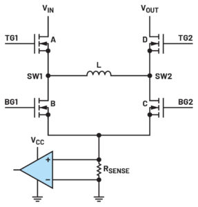
Figure 1. Ground-referenced current sensing in 4-switch buck-boost converters.
Many 4-switch buck-boost controllers require two or more current-sensing resistors to sense the I/O current and the inductor current for closed-loop operation. Analog Devices has unique buck-boost controllers that only require one current-sensing resistor to sense the current used in the current-mode control loop. Figure 1 shows a ground-referenced current-sensing method used in many traditional products. It is simple and easily implemented inside the IC. However, it can only sense the inductor current when Switch B or Switch C is turned on; this is the inductor valley current in the buck region or the peak current in the boost region, respectively. PCB layout options will be limited because the two MOSFETs (B and C) are both connected to the current-sensing resistor and must be placed close to each other.
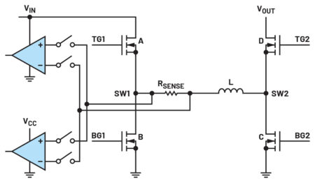
Figure 2. Switching node referred current sensing in 4-switch buck-boost converters.
Figure 2 shows a switching node referred current-sensing method used in some other buck-boost controllers. The current-sensing resistor is placed in series with the inductor, allowing it to sense the inductor current continuously. However, the voltage on the sensing resistor at the switching node swings up and down between the input voltage and ground when switches A and B are turning on/off. This requires the current-sensing circuit to have a very high common-mode rejection ratio (CMRR) to minimise the common-mode noise. Compared with tens of volts of common-mode voltage, the sensed inductor current signal is only in the range of 50mV to 100mV – a signal that could be easily distorted during power stage switching. To circumvent the noise, the current comparators are disconnected, and their inputs are turned off, as shown in Figure 2. Brief blanking times omit brief periods of inductor current information, even though the sensed signal is continuous.
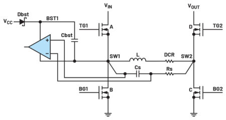
Figure 3. Inductor DCR current sensing in 4-switch buck-boost converters.
Figure 3 shows the inductor DCR current-sensing method used in the LTC7878. By matching the time constant of the RC sensing network with the inductance and the DCR (L/DCR = Rs × Cs), the inductor current is converted to a voltage signal on the sensing network (Cs) and the gain is the DCR of the inductor. The current comparator is built under the BST1/SW1 circuit, which swings together with the VIN-GND switching node during operation. Due to the same common-mode voltage on the current comparator and the switching node, the current comparator inputs do not need to disconnect from the DCR sensing signal when SW1 switches. In this way, the inductor current is cycle-by-cycle regulated and limited continuously. Compared with the switching node referred current sensing, only a single comparator under BST1/SW1 is needed. Furthermore, an option to support different DCR values and cover various inductors is provided. For inductors with small DCR, the ISNSD pin may be set to amplify the signal and improve the signal-to-noise ratio (SNR) four times larger than the conventional DCR sensing scheme. The high SNR design significantly improves system reliability and provides stable switching operation across different duty cycles.
Polyphase Parallel Operation
Inductor DCR current sensing together with continuous inductor current information allow a unified peak current mode control scheme to be implemented in the LTC7878. This scheme enables the polyphase operation, just as with many peak current mode buck or boost DC-to-DC controllers. Just by sharing all the ITH pins and daisy chaining all the CLKOUT pins, multiple LTC7878 devices can be paralleled together to supply more current to the load. The load current is distributed evenly among all the channels, and the current sharing between inductors ensures thermal balance and high efficiency. The unique cycle-by-cycle inductor current sharing reduces the overcurrent stress on the inductors during start-up and load transients, improving system reliability.
More Features
The switching frequency can be programmed between 100kHz and 600kHz or synchronised to an external clock. The integrated 7V NMOS gate drivers can drive either logic level or non-logic level MOSFETs. Other features include a smart external VCC bias pin, a PGOOD indicator pin, and selectable discontinuous conduction mode/continuous conduction mode (DCM/CCM) operation with different current limit settings. The LTC7878 can be used for inputs up to 70V and for outputs programmable from 1V to 70V and it comes in a 5mm × 5mm QFN package.
Conclusion
The LTC7878 is a high performance 4-switch buck-boost controller with inductor DCR current sensing. It uses peak current mode control in buck, boost, or buck-boost regions and always provides cycle-by-cycle peak current limits and protections. By using inductor DCR current sensing, the solution provides high efficiency while lowering component cost. To maximise the power, multiple parts can easily work in parallel in polyphase architecture.
www.analog.com
About the Author
Xu Zhang received his B.S./M.S. degrees in electrical engineering from Tsinghua University, Beijing, China, in 2000 and 2003, respectively. He received a Ph.D. degree in electrical engineering from the University of Colorado at Boulder, Boulder, CO, USA, in 2009. In early 2010, Dr. Zhang joined Analog Devices where he designed many industry-first power controller ICs such as high voltage high power charge pump controllers, the novel hybrid buck controller with switched-capacitors, bidirectional buck controllers, and 4-switch buck-boost controllers. He is now leading the Power Controller Group and responsible for developing high performance silicon-based power regulators and controllers.