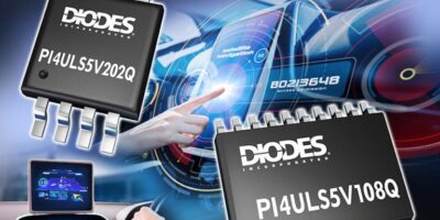
High-current photorelays achieve UL 508 for factory automation 

Certification to UL 508 for factory automation allows designers using Toshiba Electronics Europe’s photorelays to achieve UL approval for control equipment

The nine high-current photorelays in the series include low on-state resistance MOSFETs based upon Toshiba’s U-MOS VIII process that ensure high performance in a range of applications.

The TLP3556A, TLP3558A, TLP241A, TLP3543A, TLP3545A, TLP3546A, TLP3547, TLP3548 and TLP3549 are now fully certified to UL 508 and UL1577. These approvals allow designers to meet the UL safety requirements for control equipment, including the thermal design margin.

The devices can be used in industrial applications such as PLCs, interfaces and sensor control as well as building automation (heating and ventilation / heating ventilation air conditioning or HVAC). They can also be used for relay replacement in DC systems to 125V and AC systems to 400V, replacing 1-Form-A and other mechanical relays.

The photorelays are more robust than their mechanical counterparts and do not require a driver, so space, weight and cost savings can also be realised.

The nine photorelays are housed in DIP packages with four, six or eight pins (DIP4, DIP6 or DIP8). All packages have a surface mount option available, including wide-body versions. Devices are able to operate across the industrial temperature range of -40 to +85 degrees C ambient, while the case temperature can safely rise to 105 degrees C.

The photorelays can handle off-state output terminal voltages (Voff) as high as 600V. They also offer on-state resistances (Ron) as low as 22mOhm and can handle continuous currents (Ion) up to 5A. The pulsed current (IONP) is three times this level.

All nine photorelays in the range are available in production quantities.

http://www.toshiba.semicon-storage.com  

> Read More

Embedded Vision Alliance awards REAL3 image sensor as “Product of the Year”

Smartphone cameras increasingly require 3D vision capabilities as differentiating factor. Hence, Infineon Technologies developed the REAL3™ IRS2381C, a premier 3D imager sensor solution especially designed for the mobile device market.

The Embedded Vision Alliance now awarded the 3D Time-of-Flight (ToF) single chip solution as “Product of the Year” in the category “Sensors”. The Award recognises the innovation and achievement of the industry’s leading technologies, services, and products from companies enabling next generation of practical applications for computer vision.

“Congratulations to Infineon for winning Best Sensor in our 2019 Vision Product of the Year awards,” said Jeff Bier, Founder of the Embedded Vision Alliance. “Innovative sensor designs, like Infineon’s 3D Image Sensor, are enabling new 3D vision experiences such as smartphone face recognition and augmented reality. Infineon has been a pioneer in creating 3D image sensors for visual AI applications. I applaud the company’s ongoing investment in innovation and quality in this rapidly changing and often confusing market. I’m proud that Infineon is a member of the Embedded Vision Alliance and delighted they have been recognised with this outstanding honour.”

“We would like to thank the Embedded Vision Alliance for having honoured us with the ‘Product of the Year’ Award, which recognises Infineon’s innovation and performance of our REAL3™ ToF-based 3D imager the category ‘Sensors’, said Philipp von Schierstaedt, Vice President, RF & Sensors, Infineon. “Building upon the combined expertise of Infineon and pmdtechnologies, the novel sensor delivers a new level of 3D camera capabilities in mobile device applications. Infineon’s REAL3TM ToF sensor enables a unique user’s experience in secure face-authentication, computational photography and seamless AR-applications”.

Time-of-Flight (ToF) is the most advanced image sensing technology powering 3D cameras in new generation mobile devices and is posed to fuel the dramatic growth of 3D image sensing application market expected for future years. “Time-of-flight” stands for the time the photons need to travel from the camera to the subject or object of desire and back to the REAL3 sensor. Behind this concept there is unparalleled innovation: it enables the next level of highly secure user smartphone interaction.

The awarded IRS2381C image sensor ensures a high-quality, real time and secure 3D vision experience with supreme performance at all light conditions including outdoor. Compared to other 3D technologies like structured light, Infineon’s 3D ToF technology reduces the number of key components from three to two. Moreover, as distance is measured directly, it requires the least computational resources on the application processor. All this makes the application much more reliable, reduces the size and leads to more competitive costs, while enormously cutting the power drain.

Availability

The new 3D image sensor chip was developed in Graz, Dresden and Siegen and combines the know-how of Infineon’s German and Austrian locations in a single solution. With proven high volume production and a fast, in-factory enabled and lifetime valid calibration process, IRS2381C is the 3D image sensor of choice for 3D camera manufacturing in mobile device applications. More information about Infineon’s 3D image sensor family is available at www.infineon.com/real3.

> Read More

Eight-port PoE switch supports IEEE 802.3bt for smart lighting

An eight-port Power over Ethernet (PoE) switch released by Microchip guarantees 60W per port for all eight ports simultaneously. The PDS-408G PoE switch can be used for digital ceiling installations to run noiseless, fanless lighting designs.

In enterprise connected lighting applications, the PDS-408G connects separate systems such as lighting, sensors, heating ventilation and air conditioning (HVAC) and Wi-Fi access points over a single switch. Eight ports is deemed the optimal number for connected lighting and the PDS-408G can save energy and reduce operating costs, claims Microchip.

The PDS-408G complies with IEEE 802.3bt, the new PoE standard. It provides a total of 480W, including up to 90W for any individual port or 60W for eight ports simultaneously.

The PDS-408G is plenum rated and can be installed in any air handling space, and is fanless for noise-free operation in offices, hospitals and hotels. The PDS-408G also exploits PoE with safe power, simple installation, flexible deployment and remote power management features.

The PDS-408G PoE switch is available now.

Microchip offers an array of easy-to-use hardware and software tools to accelerate PoE designs, including the PIC18 PoE mainnboard, which features a PIC18 MCU, ATECC608A secure element and MIC28512 buck regulator.

https://www.microchip.com

> Read More

Software development kit streamlines SLAM in mobile devices

To develop simultaneous localisation and mapping (SLAM) –enabled mobile devices, augmented reality/virtual reality (AR/VR) headsets, robots, autonomous vehicles and drones, Ceva offers the SLAM software development kit for CEVA-XM intelligent vision DSPs and NeuPro AI processors

The kit incorporates hardware, software and interfaces that can “significantly lower the entry barrier” to integrate efficient SLAM implementations into low-power embedded systems, says Ceva.

According to Ilan Yona, vice president and general manager of the vision business unit at Ceva: “SLAM is the underlying technology that enables high-accuracy 3D mapping of a device’s surroundings”. He believes that the company’s expertise in designing vision DSPs and software algorithms will introduced customers to 3D machine vision design.

The Ceva-SLAM software development kit has a detailed interface from a CPU to offload the heavy lifting SLAM blocks to the Ceva-XM DSP. These building blocks use the DSP to support both fixed point and floating point math and extend the device’s battery life. They also include capabilities for image processing (including feature detection, feature descriptors, feature matching), linear algebra (including matrix manipulation, linear equation solving) and fast sparse equation solving for bundle adjustment. The software development kit can run a full SLAM tracking module on the Ceva-XM6 DSP at 60 frames per second consuming just 86mW (using a frame size of 1280 x 720, running on Ceva-XM6 using TSMC’s 16nm process).

The software development kit, deployed with a Ceva-XM DSP or a NeuPro AI processor, can be used for visual positioning, classical and neural network workloads for imaging and vision using SLAM.

The Ceva-SLAM software development kit is available for licensing now, exclusively in conjunction with the Ceva-XM intelligent vision DSPs and NeuPro AI processors.

Ceva will presenting the Ceva-SLAM software development kit at the Embedded Vision Summit in Santa Clara, California, USA (Wednesday 22 May).

Ceva licenses signal processing platforms and artificial intelligence processors.  It provides low power IP for vision, audio, communications and connectivity including   DSP-based platforms for LTE/LTE-A/5G baseband processing in handsets, infrastructure and cellular IoT (NB-IoT and Cat-M) enabled devices, imaging and computer vision for any camera-enabled device, audio/voice/speech and low power always-on/sensing applications for IoT markets.

http://www.ceva-dsp.com

> Read More

About Smart Cities

This news story is brought to you by smartcitieselectronics.com, the specialist site dedicated to delivering information about what’s new in the Smart City Electronics industry, with daily news updates, new products and industry news. To stay up-to-date, register to receive our weekly newsletters and keep yourself informed on the latest technology news and new products from around the globe. Simply click this link to register here: Smart Cities Registration