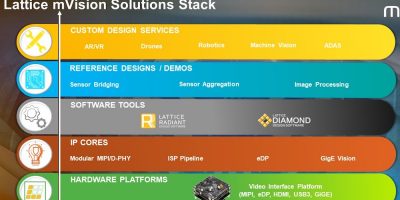
Soil sensor increases crop yield; minimises environmental damage

Incorporating three sensors in one package, a soil sensor from Murata is intended for the agricultural and horticultural industries. The sensor enables growers to increase the yield and quality of crops while experiencing lower costs associated with reduced water and fertiliser usage, explains Murata, citing these as the most important application areas for the sensor.

Murata has initiated projects using the soil sensor with partners all over the world. One example is a collaboration with Vietnam’s Can Tho University and a research project in the Mekong Delta, conducting field trials of a soil monitoring system to observe the condition of agricultural land in the delta.

Vietnam’s Mekong Delta region is subject to the salinity impact from the infiltration of seawater during the dry season as a result of a decline in the volumetric flow rate of the Mekong River, and the action of the tides under the impact of climate change driven by global warming. In addition to salt damage, the environment for agriculture has become harsher due to the increasing severity of droughts and floods.

Murata developed a compact 130mm sensor to measure the condition of agricultural land and to channel water with high precision. Using independently-developed monitoring tools environmental conditions were visualised and analysed with a view to making improvements. The sensor contributed to the implementation of IT in agriculture in the Mekong Delta region by preventing salt damage to rice paddies and orchards, ameliorating salt and sulphur contamination of agricultural land and water channels, and creating a mechanism to comprehensively manage fertilisers, crops and irrigation systems.

The sensor monitors two types of electrical conductivity (EC), temperature and the moisture content of the soil. EC level data enable growers to realise fertiliser timing, and water content of the soil for timely watering.

The sensor operates from a 3.0 to 6.5V, 50mA (maximum) supply and has an EC measurement range of 0 to 5.0dS/m with an accuracy of ± three per cent full scale. Its moisture measurement range is 0 to 60 per cent VWC at an accuracy of ± three per cent full scale, and its temperature range is -20 to 70 degrees C with an accuracy of ± one degree C.

The sensor was protected to IP68 dust and water resistance including reliable rust proofing for use in harsh environments. Interface options are UART, RS232E, RS485 and SDI-12 and maximum cable length is specified as 3m at UART, 10m at RS232E and 300m at RS485.

In the project, the wireless transmitter receiver system used consisted of a gateway, a router and several sensor nodes. Each sensor node is made up of a transmitter and three sensor units to measure the soil, field and channel water quality, and the sensing data is accumulated in the cloud. The sensor provides high-precision analysis of conditions by using a shaped sensor element and a proprietary algorithm. It is able to run for over a year of continuous operation on three size AA batteries.

http://www.murata.com

> Read More

QuickLogic partners with Nuance Communications for voice recognition

Multi-core, voice-enabled SoCs, embedded FPGA IP, and endpoint AI provider, QuickLogic is partnering with conversational AI and ambient intelligence specialist, Nuance Communications, to deliver low power, wake word and voice command technology for power-sensitive applications, such as hearable and wearable devices.

Nuance’s voice recognition technology and QuickLogic’sEOS S3 voice and sensor processing platform will provide customers an end-to-end, reliable hardware and software voice recognition solution, says QuickLogic.

The low power Nuance voice recognition technology has been integrated with QuickLogic’s advanced EOS Voice and Sensor Processing SoC. The SoC’s architecture is claimed to enable the industry’s most advanced and compute intensive sensor processing capability at a fraction of the power consumption of competing technologies.

The Nuance technology provides the performance and low power consumption required for always-on wake word detection, and specifically supports the Alexa wake-word protocol. Technical enhancements enable it to improve voice recognition accuracy in difficult or noisy environments.

The integrated system supports always-on, always-listening fixed triggers, user defined triggers and phrases, and commands that can be accurately detected in silent to extremely noisy environments.

Scott Haylock, director of product marketing at QuickLogic, explains:”In response to customer demand, and the growing hearables market, we’ve augmented the EOS S3 OPEN Software Platform to include Nuance’s technology. This addition helps QuickLogic address the largest possible product mix of new and existing voice-controlled end-products.”

The EOS S3 platform with integrated Nuance voice processing is available now.

QuickLogic is a fabless semiconductor company that develops low power, multi-core semiconductor platforms and IP for artificial intelligence (AI), voice and sensor processing. It supplies embedded FPGA IP (eFPGA) for hardware acceleration and pre-processing, and heterogeneous multi-core SoCs that integrate eFPGA with other processors and peripherals. The Analytics Toolkit provides sensor algorithms using AI technology.

http://www.quicklogic.com 

> Read More

ON Semiconductor’s digital image sensor enables AI vision systems

Intelligent vision systems for viewing and artificial intelligence (AI) can be implemented using the low power 0.3Mpixel image sensor announced by ON Semiconductor.

The ARX3A0 digital image sensor has 0.3Mpixel resolution in a 1:1 aspect ratio. It can perform like a global shutter in many conditions, with up to 360 frames per second (fps) capture rate, yet with the size, performance and response levels that relate to being a back-side illuminated (BSI) rolling shutter sensor, explains ON Semiconductor. It has a small size, square format and high frame rate, making it particularly suitable for emerging machine vision, AI and augmented reality/virtual reality (AR/VR) applications, as well as small supplemental security cameras.

To meet the demands of applications that provide still or streaming images, the ARX3A0 is designed to deliver flexible, high-performance image capture with minimal power. It consumes less than 19mW when capturing images at 30 frames per second, and just 2.5mW when capturing one frame per second.

The 1/10 in square format enables low height modules and the 3.5 mm die size helps maximise the sensor’s field of view. It can therefore be used in emerging applications where orientation is not fixed but space is limited, such as AR/VR goggles, monitoring the wearer’s eye movement. Eye movement data can be used to adjust the image viewed and possibly mitigate motion sickness. Another application is simultaneous localisation and mapping (SLAM), which can also capitalise on the ARX3A0’s size and low power.

The monochrome sensor is based on a 560 by 560 active-pixel array featuring ON Semiconductor’s NIR+ technology, giving it high sensitivity at near IR wavelengths for performance in no-light conditions or when lighting is used that is non-detectable by the human eye.

Power management features include the ability to automatically wake from a low power mode when detecting motion or lighting changes in the scene. This allows the sensor to become the main source of wake for an entire camera system saving even more system power.

Gianluca Colli, vice president and general manager, Consumer Solution Division of Image Sensor Group at ON Semiconductor said: “As we approach an era where AI is becoming an integral part of vision-based systems, it becomes clear that we now share this world with a new kind of intelligence. The ARX3A0 has been designed for that new breed of machine, where vision is as integral to their operation as it is ours.”

The ARX3A0 is available in both chip scale package and reconstructed wafer die. Evaluation boards running on ON Semiconductor’s industry leading PC-based DevWare system and prototype modules are also available through ON Semiconductor and authorised distributors.

http://www.onsemi.com

> Read More

Synopsys claims industry’s first CXL IP for data-intensive SoCs

Low latency and high bandwidth are assured for artificial intelligence (AI), memory expansion and cloud computing, says Synopsys at the introduction of its DesignWare Compute Express Link (CXL) IP.

It is, according to Synopsys, the industry’s first CXL IP for data-intensive system of chips (SoCs). The IP suite consists of controller, PHY, and verification IP for AI, memory expansion, and high-end cloud computing system-on-chips (SoCs). The CXL protocol enables low-latency data communication between the SoC and general-purpose accelerators, memory expanders, and smart I/O devices requiring high-performance, heterogenous computing for data-intensive workloads. The DesignWare CXL IP is compliant with the CXL 1.1 specification and supports all three CXL protocols (CXL.io, CXL.cache, CXL.mem) and device types to meet specific application requirements.

The CXL IP is built on Synopsys’ DesignWare IP for PCI Express 5.0, which has been adopted by semiconductor companies across all key market segments, reports the company.

“Compute Express Link is a key enabler for next-generation heterogeneous computing architectures, where CPUs and accelerators work together to deliver the most advanced solutions,” said Dr. Debendra Das Sharma, Intel Fellow and director of I/O Technology and Standards at Intel.

Synopsys’ DesignWare CXL Controller helps designers achieve timing closure at 1GHz and provides a robust 512-bit architecture that supports x16 links for maximum CXL bandwidth. The CXL controller offers reliability, availability, serviceability (RAS) capabilities to help maintain data reliability, as well as successfully debug and resolve linkup issues. The 32GTerabytes per second PHY allows more than 36dB channel loss across power, voltage and temperature (PVT) variations for long-reach applications. The VC Verification IP for CXL verifies I/O, memory access, and coherency protocol features with built-in sequences, checks, and coverage for all link configurations up to 16 lanes and 32GTbytes per second data rates. SystemVerilog test suites for CXL accelerate verification closure and are available as source code.

Synopsys’ 32G PHY IP for CXL is available now in 16-, 10-, and 7nm FinFET processes. The CXL Controller and VC Verification IP for CXL are available now.

http://www.synopsys.com/designware

> Read More

About Smart Cities

This news story is brought to you by smartcitieselectronics.com, the specialist site dedicated to delivering information about what’s new in the Smart City Electronics industry, with daily news updates, new products and industry news. To stay up-to-date, register to receive our weekly newsletters and keep yourself informed on the latest technology news and new products from around the globe. Simply click this link to register here: Smart Cities Registration