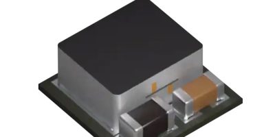
Farnell now stocks Murata’s UWB and LoRa modules

Farnell is now offering Murata’s latest UWB and LoRa connectivity modules for convenient wireless integration. These modules are designed to simplify wireless development and certification, making it easier to incorporate wireless capabilities into a wide range of applications.

Murata’s UWB modules provide high-accuracy location functionality with UWB tag and anchor functions in compact packages. These modules feature integrated RF front ends, simplifying the implementation process and reducing the need for extensive RF expertise. This allows developers to seamlessly incorporate advanced location capabilities into their applications..

Additionally, Murata’s LoRa modules offer a compact, integrated solution with an embedded MCU. Developers have the flexibility to utilise the MCU as the Host for an End Node, providing customisation possibilities for various projects.

The technology enables location accuracy in the order of 0.1m for indoor or outdoor applications. The UWB Modules available at Farnell include:

• FiRa certified UWB module, Type 2BP is the ultra small UWB module which includes NXP’s SR150 UWB chipset, clock, filters and peripheral components. Ideally suited for general IoT devices including battery operated devices.
• UWB module with integrated BLE wireless MCU, Type 2AB is designed as ultra-small, high quality and lower power consumption module. It can be operated on the wireless MCU making this a suitable part for wearables and applications where size is critical
• UWB tag module with integrated BLE wireless MCU. Type 2DK is an all-in-one UWB + Bluetooth LE combo module which integrates NXP Trimension SR040 UWB Chipset, NXP QN9090 Bluetooth LE + MCU chipset, on board antenna and peripheral components. Ideally suited for UWB Tag/Tracker which operates by coin-cell battery, and general IoT devices.

The Murata Type 1SJ LoRa Modules are some of the smallest LoRa Modules in the line-up and include the Semtech SX1262 LoRa Connect Transceiver IC and ST Microelectronics STM32L0 MCU to provide customers with a Regulatory Certified Module that can be used as the core of a LoRa End Node product design. The LoRa modules available at Farnell include:

• LoRa OpenMCU Module, Type 1SJ-295 supplied as an OpenMCU configuration to allow custom Application to be flashed to integrated MCU, together with LoRa Stack.
• LoRaWAN Modem Module, Type 1SJ-6868 pre-flashed with modem Firmware and EUI to support LoRaWAN operation by AT Commands.
• LoRa Module Evaluation Kit to support development and verification for both OpenMCU and Modem configurations of Module.

https://uk.farnell.com

> Read More

Free samples of every STMicroelectronics NPI IC available from Anglia

Anglia Components has announced a commitment to ship sample quantities of every STMicroelectronics (ST) semiconductor NPI (New Product Introduction) free of charge to customers in the UK and EU countries as part of its Anglia Live European initiative which was launched in January of this year.

John Bowman, Marketing Director at Anglia, commented: “Samples are the lifeblood of designers, and samples of NPIs are even more vital as they enable our customers to differentiate their products from those of their competitors by using the latest technology. Anglia has a long-standing relationship with ST, so we are delighted to be able to offer this service – which covers all semiconductor NPIs from the company – to the UK and European design community.”

Samples can be ordered online via Anglia’s Fast, Free, First Ezysample service available to all registered customers on Anglia Live, visit https://www.anglia-live.com

> Read More

ST BrightSense image sensor ecosystem for advanced camera performance

ST has introduced a set of plug-and-play hardware kits, evaluation camera modules and software that ease development with its ST BrightSense global-shutter image sensors. The ecosystem lets developers of mass-market industrial and consumer applications ensure superior camera performance by designing-in ST BrightSense image sensors. By sampling all pixels simultaneously, unlike a conventional rolling shutter, global-shutter sensors can capture images of fast-moving objects without distortion and significantly reduce power when coupled to a lighting system.

ST BrightSense CMOS global-shutter sensors implement advanced backside-illuminated pixel technology. Their high sensitivity enhances low-light performance and permits fast image capture, enhancing responses such as obstacle avoidance in mobile robots and face recognition in personal electronics. The sensors’ advanced 3D-stacked construction allows an extremely small die area, easing integration anywhere space is limited especially in the final optical module, while enriching the products with advanced on-chip image processing for auto-exposure, correction, and calibration. Their MIPI-CSI-2 interface makes them ideal for embedded vision and edge AI devices.

ST’s cutting-edge sensor technologies are now available in a wide variety of markets through the ST BrightSense portfolio, highlighting industrial-grade products and 10-year longevity commitment. Widespread access to these sensors now lets developers bring high-performance machine vision to applications that face strict size and power constraints and challenging operating conditions. These include factory automation, scanning, domestic and industrial robots, VR/AR equipment, traffic monitoring, and medical devices.

ST’s new mass-market offering includes evaluation camera modules that integrate image sensor, lens holder, lens, and plug-and-play flex connector to enable instant integration of the image sensors. The modules offer a selection of tiny form factors down to 5mm2, various lens options to suit different application requirements, and a plug-and-play connector that allows easy swapping. A series of hardware kits helps developers integrate the sensors with various desktop and embedded computing platforms. Complementary software tools are available for free download on ST’s website, such as a PC-based GUI and Linux drivers that assist integration with popular processing platforms including STM32MP2 microprocessors.

The ST BrightSense global-shutter family currently comprises the VD55G0, VD55G1, and VD56G3 monochrome sensors with resolution from 0.38Mpixel to 1.5Mpixel, as well as the color VD66GY with 1.5Mpixel. The sensors, along with their evaluation camera modules, and development boards are in production now.

https://www.st.com/brightsense

> Read More

Intel announces first fully integrated optical I/O chiplet

Intel’s Integrated Photonics Solutions (IPS) Group has announced the industry’s most advanced and first-ever fully integrated optical compute interconnect (OCI) chiplet co-packaged with an Intel CPU and running live data. Intel’s OCI chiplet represents a leap forward in high-bandwidth interconnect by enabling co-packaged optical input/output (I/O) in emerging AI infrastructure for data centres and high performance computing (HPC) applications.
This first OCI chiplet is designed to support 64 channels of 32 gigabits per second (Gbps) data transmission in each direction on up to 100 meters of fibre optics and is expected to address AI infrastructure’s growing demands for higher bandwidth, lower power consumption and longer reach. It enables future scalability of CPU/GPU cluster connectivity and novel compute architectures, including coherent memory expansion and resource disaggregation.
AI-based applications are increasingly deployed globally, and recent developments in large language models (LLM) and generative AI are accelerating that trend. Larger and more efficient machine learning (ML) models will play a key role in addressing the emerging requirements of AI acceleration workloads. The need to scale future computing platforms for AI is driving exponential growth in I/O bandwidth and longer reach to support larger processing unit (CPU/GPU/IPU) clusters and architectures with more efficient resource utilisation, such as xPU disaggregation and memory pooling.
Electrical I/O supports high bandwidth density and low power, but only offers short reaches of about one meter or less. Pluggable optical transceiver modules used in data centres and early AI clusters can increase reach at cost and power levels that are not sustainable with the scaling requirements of AI workloads. A co-packaged xPU optical I/O solution can support higher bandwidths with improved power efficiency, low latency and longer reach – exactly what AI/ML infrastructure scaling requires.
The fully Integrated OCI chiplet leverages Intel’s silicon photonics technology and integrates a silicon photonics integrated circuit (PIC), which includes on-chip lasers and optical amplifiers, with an electrical IC. The OCI chiplet demonstrated at OFC was co-packaged with an Intel CPU but can also be integrated with next-generation CPUs, GPUs, IPUs and other system-on-chips (SoCs).
This first OCI implementation supports up to 4 terabits per second (Tbps) bidirectional data transfer, compatible with peripheral component interconnect express (PCIe) Gen5. The live optical link demonstration showcases a transmitter (Tx) and receiver (Rx) connection between two CPU platforms over a single-mode fibre (SMF) patch cord. The CPUs generated and measured the optical Bit Error Rate (BER), and the demo showcases the Tx optical spectrum with 8 wavelengths at 200 gigahertz (GHz) spacing on a single fibre, along with a 32 Gbps Tx eye diagram illustrating strong signal quality.
The current chiplet supports 64 channels of 32 Gbps data in each direction up to 100 meters (though practical applications may be limited to tens of meters due to time-of-flight latency), utilising eight fibre pairs, each carrying eight dense wavelength division multiplexing (DWDM) wavelengths. The co-packaged solution is also remarkably energy efficient, consuming only 5 pico-Joules (pJ) per bit compared to pluggable optical transceiver modules at about 15 pJ/bit. This level of hyper-efficiency is critical for data centres and high-performance computing environments and could help address AI’s unsustainable power requirements.
These PICs were packaged in pluggable transceiver modules, deployed in large data centre networks at major hyperscale cloud service providers for 100, 200, and 400 Gbps applications. Next generation, 200G/lane PICs to support emerging 800 Gbps and 1.6 Tbps applications are under development.
Intel is also implementing a new silicon photonics fab process node with state-of-the-art device performance, higher density, better coupling and vastly improved economics. Intel continues to make advancements in on-chip laser and semiconductor optical amplifier (SOA) performance, cost (greater than 40% die area reduction) and power (greater than 15% reduction).

https://www.intel.com/

> Read More

About Smart Cities

This news story is brought to you by smartcitieselectronics.com, the specialist site dedicated to delivering information about what’s new in the Smart City Electronics industry, with daily news updates, new products and industry news. To stay up-to-date, register to receive our weekly newsletters and keep yourself informed on the latest technology news and new products from around the globe. Simply click this link to register here: Smart Cities Registration