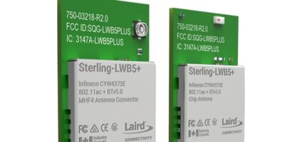
SGET announces postage stamp CoM standard

Credit card sized embedded computer modules have a new footprint that reduces the size of a computer on module (COM) to a postage stamp. Technical consortium, SGET, has announced release 1.0 of the Open Standard Module (OSM) COM standard. OSM defines one of the first standards for directly solderable and scalable embedded computer modules.

The new specification aims to standardise the footprint and interface set of low-power application processors based on MCU32, Arm and x86 architectures across different sockets, manufacturers and architectures. Target applications of the new module standard include IoT-connected embedded, IoT, and edge systems that run open-source operating systems and are used in harsh industrial environments.

“OSM modules give ODMs and OEMs a miniature form factor with high scalability” explained Martin Unverdorben, chairman of the SGET STD.05 Standard Development Team. The modules are application-ready and supplied with all necessary software drivers and board support packages. The specification is open source, both in terms of the hardware and software, he added.

Like all CoM standards, OSMs simplify and accelerate the design-in of processors. At the same time, applications become processor-agnostic, which makes them scalable and future-proof, says SGET. They also protect NRE investments and extend the long-term availability, to increase RoI and sustainability of embedded systems. The OSM specification offers an extra level of ruggedness due to the BGA design and automated surface mount technology (SMT), which can further reduce production costs in series production, advises SGET.

OSMs are also published and licensed under Creative Commons Plus (CC+) dual license. This allows an open licensing model, such as the Creative Commons Attribution-ShareAlike license (CC B-SA 4.0) for a defined set of materials, components and software, and a commercial license for everything not included in this set. This ensures that development data, such as block diagrams, libraries and BOMs resulting from the development of OSMs, will be publicly available. It is also possible to license the IP of a carrier board design commercially without violating the open source idea.

The new OSM specification expands the portfolio of SGET module specifications with solderable BGA mini modules that are “significantly smaller” than previously available modules. The largest OSM measures 45 x 45mm, making it 28 per cent smaller than the µQseven module (40 x 70mm) and 51 per cent smaller than SMARC (82 x 50mm).

Other sizes are OSM Size-0 (30 x 15mm) with 188 BGA pins, OSM Size-S (30 x 30mm) with 332 pins, OSM Size-M (30 x 45mm) and 476 pins and Size-L (45 x 45mm) with 662 BGA pins. SMARC, by comparison, specifies 314 pins and Qseven 230. The BGA design makes it possible to implement significantly more interfaces on a smaller footprint, points out SGET, both in terms of miniaturisation and the increasing complexity of requirements.

The interfaces vary in type and design depending on the size of the OSM modules. Modules from Size-S upwards offer video interfaces for up to one RGB and four-channel DSI. Size-M modules can additionally support two eDP/eDP++, and Size-L adds an LVDS interface for graphics.

The OSM specification provisions up to five Ethernet for system-to-system communication. In addition, all modules have what is called a communication area, providing 18 pins for antenna signals for wireless communication or the integration of field buses. There are four USB 2.0 or two USB 3.0 (only in Size-L), up to two CAN, and four UART. Flash storage media can be connected via UFS. Up to 19 pins are available for manufacturer-specific signals. There are 39 general purpose I/Os, SPI, I2C, I2S, SDIO and two analogue inputs. Up to 58 pins are reserved for future purposes.

https://sget.org

> Read More

Radar sensor suite has all-round sensing for vehicles

Sensing to cover all radar segments from Europe’s NCAP (New Car Assessment Programme) to 4D imaging radar is provided by a suite of automotive radar sensor chipset suite by NXP.

The NXP radar sensors are built on 16nm FinFET and 40nm RFCMOS technology. The include the RFCMOS 77GHz radar transceivers, the S32R45 high-performance radar processors for imaging radar and the S32R294 radar processor for corner and front radar applications

The processors and transceivers offer automotive manufacturers flexible and scalable configurations that address NCAP requirements for corner and front radar applications as well as what is claimed to be the first commercially viable path to volume production for 4D imaging radar.

4D imaging radar expands radar’s capabilities from measuring range and speed to include direction, angle of arrival, and elevation measurement.

NXP offers imaging radar, which “significantly enhances radar’s performance”. It delivers multi-modal capabilities and extends today’s L2+ features, such as highway pilot and lane change assistance, by offering very high resolution images for precise environmental mapping and scene understanding. This is an important part of enabling full autonomy in urban settings, says NXP.

NXP’s new purpose-built S32R45 radar processor and the TEF82xx transceivers deliver the fine angular resolution, processing power and range required to distinguish between small objects in the distance and separate and classify vehicles and vulnerable road users (e.g. cyclists or pedestrians) in crowded environments. This capability is targeted at providing better driving decisions.

The suite also provides scalability for long-range front radar and advanced multi-mode use cases, e.g. simultaneous blind-spot detection, lane change assistance and elevation sensing. These advanced applications require extended range and significantly enhanced angular resolution to detect and separate multiple objects simultaneously. The new S32R294 radar processors, combined with the NXP TEF82xx transceivers provide a scalable solution to address NCAP, advanced corner radar and long-range front radar sensor requirements. They can also be tailored for individual use cases.

“Radar has evolved from just detecting other cars’ velocity and distance to providing imaging radar’s high-resolution object and feature detection for precisely mapping the car’s surroundings,” said Torsten Lehmann, executive vice president and general manager, Radio Frequency Processing, NXP.

NXP claims to be the first company to broadly deliver 77GHz RFCMOS radar technology in high volume, mass production and says it helps customers optimise the total cost of ownership with scalable, re-useable radar systems.

Target applications are in traditional automotive manufacturers, focused on automated driving levels one to three, and for mobility as service innovators developing robotaxi and safe delivery applications for levels four and five automation.

The devices are sampling now, with mass production expected in 2021.

http://www.nxp.com

> Read More

Mach-NX FPGA is designed for cyber-resilient systems

Lattice Semiconductor has added support for ECC 384 and SPDM protocols in its second generation of secure control FPGAs. Following on from the secure control of the Lattice MachXO3D FPGAs, released last year, the FPGAs are the third family in 12 months that have been developed on the Lattice Nexus FPGA platform. The company says the Mach-NX FPGAs deliver heightened security features and the fast, power-efficient processing needed to implement a real time hardware root of trust (HRoT) on future server platforms, computing, communications, industrial and automotive systems.

According to the company, the Mach FPGA families can simplify and accelerate implementation of technologies, such as ECC 384 and data security protocols like SPDM, to secure platforms against cyber attack and IP theft.

Esam Elashmawi, chief strategy and marketing officer at Lattice, commented: “Securing systems against unauthorised firmware access goes beyond establishing a HRoT at boot. It also requires that components used to build the system are not compromised as they move through the global supply chain. When combined with the additional protection afforded by our SupplyGuard security service, Lattice Mach-NX FPGAs can protect a system throughout its entire lifecycle: beginning at the time components start moving through the supply chain, through initial product assembly, end-product shipping, integration, and throughout the product’s operational lifetime.”

The Mach-NX FPGAs combine a secure enclave (a 384-bit hardware-based crypto engine supporting reprogrammable bitstream protection) with a logic cell and I/O block. The enclave helps secure firmware, and the logic cell and I/O block enable system control functions such as power management and fan control. The FPGAs can verify and install the over-the-air firmware updates to keep systems compliant as security guidelines evolve and protocols are introduced.

The parallel processing architecture and dual-boot flash memory configuration provide the near instantaneous response times needed to detect and recover from attacks (a level of performance beyond the capabilities of other HRoT platforms like MCUs), reports Lattice.

The FPGAs will support Lattice Sentry, a software stack of customisable embedded software, reference designs, IP and development tools. This accelerates the implementation of secure systems to comply with NIST SP-800-193, Platform Firmware Resiliency (PFR) guidelines and MCTP-SPDM.

The Lattice SupplyGuard supply chain security subscription service tracks locked Lattice FPGAs through their entire lifecycle, from the point of manufacture, through transport via the global supply chain, system integration and assembly, initial configuration, and deployment.

The Lattice Propel design environment accelerates design of a customised, PFR-compliant HRoT solution. It uses a GUI-based development environment that allows developers to create PFR solutions while minimising the need to write RTL code, explains Lattice.

http://www.latticesemi.com

> Read More

TDK uses proprietary microcontroller in flash storage disks

Five series of flash storage products from TDK use GBDriver GS2, its proprietary NAND flash memory control IC, which supports serial ATA. They are optimised for industrial, medical, smart grid, transportation and security applications.

As 3D flash memory technology advances, flash storage solutions with capacities over 1 Tbyte are widely used, but data reliability requirements continue to become more sophisticated, explains TDK. With flash storage integrated into edge devices in industrial equipment, and other industrial IoT devices mostly used to store OS or device applications, the demand has increased for highly reliable storage devices that also protect user data.

In addition to auto refresh and data recovery features, the GBDriver GS2 features new error code correction (ECC), the LDPC memory and strong RAID features, and enhances data reliability, says TDK. The five families provide a wide range of storage capacities, from 16Gbyte to 1.6Tbyte.

A standard feature of all five storage products is the internal power back-up protection circuits, with 2D MLC NAND flash memory. There is also write protection with unified write filter (UWF) for Windows 10. Power interruption tolerance is also enhanced with 3D TLC NAND flash memory.

They also offer strengthened security features, including a new firmware anti-tampering feature. TDK’s original anti-spoofing security feature, AES128/256-bit encryption, and ATA security, protects users against falsification and the leakage of data stored in NAND flash memory.

They storage disks can be used in a variety of industrial IoT applications, including in devices such as information terminals and edge computing systems. They are also suitable for industrial computers, factory automation equipment, railway and transportation service equipment. Other uses are in ticket vending machines and banking terminals, medical and data analysis equipment, smart grid equipment and security equipment, for example in security terminals.

TDK Corporation was established in 1935 to commercialise ferrite, a key material in electronic and magnetic products. TDK’s portfolio features passive components such as ceramic, aluminum electrolytic and film capacitors, as well as magnetics, high-frequency, and piezo and protection devices. The product spectrum also includes sensors and sensor systems such as temperature and pressure, magnetic, and MEMS sensors. In addition, TDK provides power supplies and energy devices and magnetic heads.

The products are marketed under the product brands TDK, Epcos, InvenSense, Micronas, Tronics and TDK-Lambda.

TDK focuses on demanding markets in automotive, industrial and consumer electronics, and information and communication technology. The company has a network of design and manufacturing locations and sales offices in Asia, Europe, and in North and South America.

http://www.tdk.com

> Read More

About Smart Cities

This news story is brought to you by smartcitieselectronics.com, the specialist site dedicated to delivering information about what’s new in the Smart City Electronics industry, with daily news updates, new products and industry news. To stay up-to-date, register to receive our weekly newsletters and keep yourself informed on the latest technology news and new products from around the globe. Simply click this link to register here: Smart Cities Registration