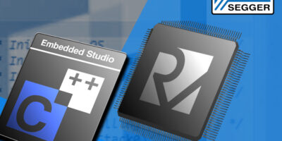
Synopsys packages controller, PHY and verification IP in HBM3 suite

To accelerate development of 2.5D multi-die package systems, Synopsys offers what is claims is the industry’s first complete HBM3 IP and verification for high-performance computing, artificial intelligence (AI) and graphics SoCs.

The DesignWare HBM3 controller and PHY IP are built on silicon-proven HBM2E IP, and use Synopsys’ interposer technology to enable high memory bandwidth at up to 921Gbytes per second.

The verification solution includes verification IP with built-in coverage and verification plans, off-the-shelf HBM3 memory models for ZeBu emulation, and HAPS prototyping system, accelerates verification from HBM3 IP to SoCs.

3DIC Compiler multi-die design offers architectural exploration, implementation and system-level analysis. The DesignWare HBM3 controller IP supports a variety of HBM3-based systems with flexible configuration options. The controller minimises latency and optimises data integrity with advanced RAS (reliability, availability, serviceability) features that include error correction code, refresh management and parity.

The DesignWare HBM3 PHY IP in 5.0nm process, is available as pre-hardened or customer configurable PHY. It operates at up to 7200Mbits per second per pin and is claimed to “significantly” improve power efficiency and supports up to four active operating states enabling dynamic frequency scaling. The DesignWare HBM3 PHY uses an optimised micro bump array to help minimise area. The support for interposer trace lengths gives designers more flexibility in the PHY placement without impacting performance.

Synopsys Verification IP for HBM3 uses next-generation native SystemVerilog Universal Verification Methodology architecture to integrate existing verification environments and run a greater number of tests, accelerating time to first test. The off-the-shelf HBM3 memory models for ZeBu emulation and HAPS prototyping system enable RTL and software verification for higher levels of performance.

The suite has already been welcomed by customers. “Micron is committed to empowering the world’s most advanced computing systems with the industry’s highest performing solutions. HBM3 will deliver the memory bandwidth critical to enabling the next generation of high-performance computing and artificial intelligence systems,” said Mark Montierth, Micron vice president and general manager of High-Performance Memory and Networking.

“SK hynix, a leading global semiconductor manufacturer, continues to invest in developing next-generation memory technologies, including HBM3 DRAMs, to meet the exponential growth in workloads for AI and graphics applications,” said Cheol Kyu Park, vice president, HBM Product Champion and head of DRAM Product Engineering at SK hynix. “We will leverage our long-standing relationship with Synopsys to provide our mutual customers with fully-tested and interoperable HBM3 solutions that can maximize memory performance, capacity and throughput.”

“Our recent collaboration with Synopsys, leveraging Synopsys’ HBM2E IP on 5nm process and integrated full-system multi-die design platform, will extend to include the new DesignWare HBM3 IP and verification solutions. As a result, our customers can achieve higher memory performance and capacity in SoCs requiring the upcoming HBM3 specification,” added Yutaka Hayashi, vice president of Data Center & Networking Business Unit at Socionext

The DesignWare IP includes logic libraries, embedded memories, PVT sensors, embedded test, analogue IP, interface IP, security IP, embedded processors and subsystems. To accelerate prototyping, software development and integration of IP into SoCs, Synopsys’ IP Accelerated initiative offers IP prototyping kits, IP software development kits and IP subsystems.

The DesignWare HBM3 Controller, PHY, and Verification IP as well as the ZeBu emulation memory model, HAPS prototyping system and 3DIC Compiler are available now.

http://www.synopsys.com

> Read More

Automotive gateway solution based on R-Car S4 SoCs and PMICs

An automotive gateway solution with R-Car S4 system on chips (SoCs) and power management ICs (PMICs) for next-generation vehicle computers, communication gateways, domain servers and application has been launched by Renesas. The new solution meets the automotive industry’s requirements for high performance, high-speed networking, high-security and high-functional safety levels that are required as E/E architectures evolve into domains and zones. The solution enables software reusability and includes the new best-in-class PMICs designed to work seamlessly with the R-Car S4.

The Renesas R-Car S4 is one of the first products in Renesas’ 4th-generation R-Car family. It includes multiple Arm Cortex A55, Cortex R52 and the company says it is the first to implement an RH850 MCU for control domain management. R-Car S4 SoCs offer automotive interfaces such as 16x CAN FD, 16x LIN, 8x SENT, 1x FlexRay, 4x PCIe V4.0 and also a high-bandwidth 3 x 2.5Gbit ethernet switch to enable rich communication and connectivity options inside and outside the vehicle.

This automotive solution means designers can re-use up to 88 per cent of software code developed for third generation R-Car SoC and RH850 MCU applications. The software package supports R-Car S4 application development including the real-time cores with various drivers and basic software such as Linux BSP and hypervisors. In addition, a virtual platform is available from a partner company enabling early software development and evaluation to help reduce design time and cost.

The new PMICs provide advanced power modes that support low power operation. The RAA271041 PMIC accepts the vehicle’s 12V supply and supports wide operation for load dump and cold cranking pulses while providing the first-stage regulation. The RAA271005 is a Safe 11-channel PMIC that takes the RAA271041’s output and steps it down further to the various supply voltages needed by R-Car S4 and its peripherals such as LPDDR4x memory. The RAA271041 and RAA271005 PMICs provide a complete power solution from vehicle battery down to system voltage.

For more information go to https://www.renesas.com/products/automotive-products

> Read More

i.MX 8XLite applications processor focus on secure V2X and industrial IoT applications

From NXP Semiconductors comes the release of the i.MX 8XLite applications processor focused on secure V2X and industrial Internet of Things (IoT) applications. The SoC features NXP’s integrated EdgeLock security and is targeted at meeting FIPS 140-3 while simultaneously executing complex cryptography and processing telematics data.

FIPS 140-3 is a US government security standard for cryptographic modules used in various applications, including V2X and critical infrastructure applications.

The applications processor offers carmakers the opportunity to expand V2X benefits to entry level vehicles. It enables fleet management for automated vehicles and, says NXP, reduces operational costs via enhanced traffic control, improved traffic flow and optimised path planning. Industrial IoT developers can leverage the SoC in secure wireless, Ethernet and control area networking applications such as industrial vehicle management, building control and safety systems, solar power generation, EV charging stations and access controllers.

The i.MX 8XLite SoC is a member of the i.MX 8 series of applications processors, purpose-built with a V2X accelerator, which can be leveraged as part of NXP’s RoadLink V2X solution or as a standalone accelerator. Its vehicle-to-infrastructure capability helps vehicles communicate with roads, bridges and roadside units to obtain information about road conditions ahead. Its car-to-car communication enables cars to communicate via wireless technologies such as IEEE® 802.11p, 5G and cellular, creating a network of similarly equipped vehicles to “see” further ahead.

“We believe road safety is for everyone, and it should scale across vehicles and devices,” said Dan Loop, general manager, automotive edge processing, NXP. “The i.MX 8XLite SoC offers the security and performance needed to expand the safety benefits of V2X into entry level vehicles and into exciting new realms of unmanned industrial delivery and drone applications.”

NXP Semiconductors is driving innovation in the automotive, industrial and IoT, mobile, and communication infrastructure markets. Built on more than 60 years of combined experience and expertise, the company has approximately 29,000 employees in more than 30 countries and posted revenue of $8.61 billion in 2020.

For more information go to http://nxp.com/iMX8XLite

> Read More

TDK offers miniaturised, highly sensitive MEMS pressure sensor element

Designed to measure a range of 0 to 100 mbar, TDK Corporation’s C35 type pressure sensor element combines high sensitivity with low dimensions of 2.05 x 2.05 x 1.2 mm, enabling compact pressure sensor designs.

The pressure sensor element with ordering code B58601E35 works according to the piezoresistive principle via a Wheatstone bridge and is certified for an operating voltage of up to 10 V.

Offering a high sensitivity of 110 mV/V/bar, C35 is suitable for applications with high demands of sensitivity, accuracy and long-term stability of 0.1% FSON.

Furthermore, C35 is designed for a wide temperature range from -40 degrees C to +150 degrees C and is suitable for pressure measurements of non-aggressive gases and liquids. The main uses are in applications that require high reliability and extremely precise pressure measurement, such as medical engineering and the industrial and automotive sectors.

TDK Corporation is a leader in electronic solutions for the smart society based in Tokyo, Japan. It was established in 1935 to market ferrite, a key material in electronic and magnetic products.

The company’s portfolio features passive components such as ceramic, aluminum electrolytic and film capacitors, as well as magnetics, high-frequency, and piezo and protection devices. The range of products also includes sensors and sensor systems such as temperature and pressure, magnetic and MEMS sensors.

In addition, TDK provides power supplies and energy devices and magnetic heads. These products are marketed under the product brands TDK, EPCOS, InvenSense, Micronas, Tronics and TDK-Lambda.

TDK focuses on demanding markets in automotive, industrial and consumer electronics, and information and communication technology. The company has a network of design and manufacturing locations and sales offices in Asia, Europe, and in North and South America.

In fiscal 2021, TDK posted total sales of $13.3 billion and employed about 129,000 people worldwide.

For more information go to

https://www.tdk-electronics.tdk.com/en/pressure_sensor_elements

> Read More

About Smart Cities

This news story is brought to you by smartcitieselectronics.com, the specialist site dedicated to delivering information about what’s new in the Smart City Electronics industry, with daily news updates, new products and industry news. To stay up-to-date, register to receive our weekly newsletters and keep yourself informed on the latest technology news and new products from around the globe. Simply click this link to register here: Smart Cities Registration