Multi-layer chip antennas have been added to the range available from Würth Elektronik, contributing to the miniaturisation of radio applications.
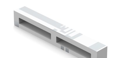
Measuring just 40 x 6.0 x 5.0mm, the WE-MCA antenna (7488918022) covers the 700 to 960MHz and 1710 to 2690MHz frequency ranges. The form factor and slender profile mean the antenna offers an “excellent size-to-performance ratio”, said Würth.
WE-MCA is suited for applications such as GSM 900, WLAN / WiFi, Bluetooth, GPS / GNSS, ZigBee, and mobile communication (4G / LTE). Würth Elektronik offers products for the development of radio applications, including a variety of radio modules and EMC products for high frequency applications, in particular compact IoT and smart building applications. The chip antennas are robust, with an operating temperature range from -40 to +85 degrees C.
To help customers with the layout of miniaturised radio applications and the selection of suitable inductors and capacitors, Würth Elektronik offers antenna matching and characterisation support for its range of multi-layer chip antennas.
The WE-MCA chip antennas are supplied packaged in reels for surface mount assembly, with no restrictions regarding the number of items. Free-of-charge samples are available on request.
Würth Elektronik eiSos Group is a manufacturer of electronic and electromechanical components for the electronics industry. Würth Elektronik eiSos is one of the largest European manufacturers of passive components and is active in 50 countries. Production sites in Europe, Asia and North America supply a growing number of customers worldwide.
The product range includes EMC components, inductors, transformers, RF components, varistors, capacitors, resistors, quartz crystals, oscillators, power modules, wireless power transfer, LEDs, sensors, connectors, power supply elements, switches, push-buttons, connection technology, fuse holders and solutions for wireless data transmission.
Würth Elektronik is part of the Würth Group, specialising in assembly and fastening technology.