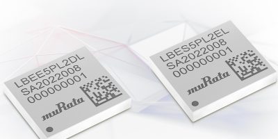
Low power cascadable gain blocks can be used in 4G/5G infrastructure

The CMX90G301 and CMX90G302 low power cascadable gain blocks have positive gain-slopes of +1dB and +2dB respectively and an operating frequency range of 1.4 to 7.1GHz. Both devices are suitable for a range of RF applications, including 4G/5G infrastructure and devices operating in unlicensed frequency bands, advised CML Microcircuits.

The CMX90G301 and CMX90G302 positive gain slope amplifiers were developed using CML’s SµRF RFIC / MMIC design capability. These general-purpose gain blocks use GaAs pHEMT technology to achieve an optimal combination of low DC power, low noise, and high gain. 

The CMX90G301 has +1dB positive gain slope, while the CMX90G302 offers a +2dB gain slope for applications requiring more gain slope compensation. Both devices deliver a small signal gain of 14.8 to 16.0dB, a P1dB output rating of +11.5dBm at 3.5 GHz and a low noise figure of 2dB.

As is the case with other devices in the SµRF family, the CMX90G301 and CMX90G302 gain blocks have a high level of integration and support minimised component counts and reduced PCB footprints, said CML. The two cascadable, gain blocks eliminate the need for passive equalisation circuits within the system design. An on-board active bias circuit allows the devices to operate over a wide supply voltage of 2.7 to 5V, with a typical current of 22mA. The RF ports of each device are matched to 50 Ohm, which supports rapid product development cycles, particularly for mass-market applications, said the company.

The CMX90G301 and CMX90G302 address the growing market requirement for high-performing mmWave devices, said Matthew White, marketing manager, RF and mmWave. 

CML Microcircuits is a world-leader in the design, development and supply of low power analogue, digital and mixed-signal semiconductors for telecommunications systems globally.

The company’s varied portfolio means that CML devices are used in an extensive range of industrial and commercial products for licensed and unlicensed wireless voice and data systems.

SµRF is a CML Microcircuits product portfolio of RF front end components with design capability from 1.0 to 100GHz.

In addition to a range of devices, the company is able to offer bespoke solutions to customers. This service includes design assistance, advice, and first-class technical support.

http://www.cmlmicro.com 

> Read More

NXP releases RFCMOS radar transceivers for ADAS and AD

Second generation radar transceivers from NXP are now available for ADAS (advanced driver assistance systems) and AD (autonomous driving). The TEF82xx series of 77GHz RFCMOS radar transceivers is optimised for fast chirp modulation, and supports short-, medium- and long-range radar applications, including cascaded high-resolution imaging radar. 

It enables 360 degree sensing for critical safety applications, including automated emergency braking, adaptive cruise control, blind-spot monitoring, cross-traffic alert and automated parking.

Radar is used for sensing in passenger vehicles’ ADAS but also in MaaS (mobility as a service) applications, says NXP. Fully autonomous driving will demand higher RF performance for distances beyond 300m, as well as at finer resolutions down to sub-degree level to accurately detect, separate and classify smaller objects. Used with NXP’s scalable family of S32R radar processors, NXP said the TEF82xx RFCMOS radar transceivers are able to deliver the fine angular resolution, processing power, and ranges, required for production-ready imaging radar solutions.

The RFCMOS transceivers have three transmitters, four receivers, ADC conversion, phase rotator and low phase noise VCOs (voltage controlled oscillators). It also includes built-in safety monitors and external interface capability for MIPI-CSI2 and LVDS and complies with ISO26262 and ASIL Level B standards.

NXP has doubled RF performance compared with the first generation devices, with improvements such as a +6dB phase noise improvement, output power of 14dBm at phase noise of -95dBc/Hz and a receiver noise figure of 11.5dB. TEF82xx transceivers use a compact eWLB package with exposed die, which optimises heat transfer to meet demanding thermal conditions, even at elevated ambient temperatures. A particularly short chirp return time of just four microseconds reduces power on time to reduce sensor power consumption. It also allows chirps to be spaced more closely in time which increases speed estimation capabilities.

Developers can easily build and optimise applications using the radar algorithm library offered by the automotive-grade radar software development kit (RSDK) without having to spend time manually fine-tuning accelerator software. There is also a large ecosystem of compilers, development environments, MCALs, and both free and commercial RTOS support.

http://www.nxp.com

> Read More

ClockMatrix delivers Class D compliance for O-RAN S-plane Requirements

The 8A34001 system synchroniser is part of Renesas’ ClockMatrix family of precision timing. It is used in AMD’s Zynq UltraScale+ RFSoC DFE ZCU670 evaluation kit and reference design for 5G New Radio (5G NR) and generates low jitter, precision timing signals based on the IEEE 1588 precision time protocol (PTP) and synchronous Ethernet (SyncE).

It exceeds next-generation 5G radio requirements including synchronisation and offers full ITU-T G.8273.2 T-BC/T-TSC class C and D compliance. Renesas offers open source SYNCE4L and PCM4L, that is built on open source PTP4L, and device drivers already in a Linux kernel for the 8A34001. Alternative solutions rely on proprietary software that can be difficult for end customers to integrate and customise on to their software platforms.

The AMD ZCU670 is an evaluation and development platform based on Zynq UltraScale+ RFSoC DFE, the latest AMD silicon for 5G NR targeting both FR1 and FR2 (mmWave) O-RAN applications. 

The 8A34001 performance has been verified on the ZCU670 evaluation platform and has been shown to exceed the 5G system requirements, reported Renesas. The relevant compliance reports and test results are available from Renesas on request. The 8A34001 system synchroniser will be made available as part of the AMD O-RAN reference design where it is used to implement the S-plane functionality in an O-RU reference design. 

Renesas offers a broad silicon timing portfolio in the industry, including a wide range of buffers, oscillators and clock synthesiser products, to resolve timing challenges in wireless infrastructure, networking, data centres and consumer applications. 

The AMD Zynq UltraScale+ RFSoC DFE ZCU670 evaluation kit is available today for qualified customers. The entire ClockMatrix family of timing devices is available from Renesas and its authorised distributors. 

http://www.renesas.com 

> Read More

SiC based modules increase range, with faster charging for EVs

Automotive silicon-carbide (SiC) -based power modules, the AMP32 series, have been developed by onsemi for on-board chargers. The modules, claimed the company, enable faster charging and increased range for all types of electrical vehicles.

The three APM32 SiC-based power modules feature transfer moulded technology and are intended for use in on-board charging and high voltage (HV) DC/DC conversion in all types of electric vehicles (xEV). The modules are specifically designed for high-power 11 to 22kW on-board chargers.

Each module exhibits low conduction and switching losses, said onsemi, “best in class thermal resistance” and high voltage isolation to deal with 800V bus voltage. The enhanced efficiency and lower heat generation allow one OBC to charge the EV faster and increase its operating range, claimed the company.

The modules allow designers to meet charging efficiency and space goals, said onsemi. “By adopting the pre-configured modular format, designers are able to configure their designs faster, with significantly lower time to market and design risk,” said Fabio Necco, vice president and general manager, automotive power solutions at onsemi.

Each APM32 module is serialised for full traceability. The modules can operate with junction temperatures (Tj) up to 175°C, for reliable operation even in challenging, space-constrained automotive applications.

Two modules, the NVXK2TR40WXT and NVXK2TR80WDT, are configured in H-bridge topology with a breakdown (V(BR)DSS) capability of 1200V, ensuring suitability for high voltage battery stacks. They are designed to be used in the OBC and HV DC/DC conversion stages. The third module, the NVXK2KR80WDT, is configured in Vienna rectifier topology and used in the power factor correction (PFC) stage of the OBC. 

All three modules are housed in a compact dual inline package (DIP), which is claimed to ensure low module resistance. The top cool and isolated features meet stringent automotive industry standards, the creepage and clearance distances meet IEC 60664-1 and IEC 60950-1. Additionally, the modules are qualified to AEC-Q101 and AQG 324.

The company also announced that it will introduce a six-pack and full-bridge modules. 

http://www.onsemi.com

> Read More

About Smart Cities

This news story is brought to you by smartcitieselectronics.com, the specialist site dedicated to delivering information about what’s new in the Smart City Electronics industry, with daily news updates, new products and industry news. To stay up-to-date, register to receive our weekly newsletters and keep yourself informed on the latest technology news and new products from around the globe. Simply click this link to register here: Smart Cities Registration