Automated testing software provides insightful analytics to improve sensor design and performance, said Keysight Technologies. The company has expanded its portfolio of autonomous driving validation test products with the E8717A lidar target simulator (LTS), which enables automakers and lidar sensor makers to test and validate lidar sensors for autonomous vehicles (AVs).
Initially developed for use in meteorology and topography, lidar is now being adopted as an automotive sensing technology that enables AVs to “see” and safely navigate through complex driving scenarios. Lidar sensor makers must ensure advanced driver assistance systems (ADAS) quickly and reliably detect objects. To properly test sensors, designers currently need large floor spaces and use traditional target boards. There is also industrial pressures to reduce sensor cost and scale to mass production, said Keysight.
The Keysight LTS addresses these challenges by simulating test targets at defined distances and reflectivity with a compact and standardised bench setup. It is designed to simplify and accelerate the testing, validation and production of automotive lidar sensors through standardisation and automation.
The compact bench setup saves test floor space by simulating target distances from three to 300 metres and simulating surface reflectivity from 10 to 94 per cent.
The testing software generates insightful analytics by sweeping target distance and reflectivity. This enables the design and performance of sensors to be improved, said Keysight.
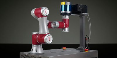
The LTS test setup is fully automated using a cobot and powered by Keysight PathWave Test Executive for Manufacturing for test automation. The cobot provides precise device movement for field of view testing and the automation software accelerates testing and throughput to support volume production.
According to Thomas Goetzl, vice president and general manager for Keysight’s Automotive and Energy Solutions, this is the first cobot-assisted lidar target simulator with variable distance and reflectivity simulation available and enables the company to “support a volume roll out of lidar with a scalable manufacturing test solution.”
Keysight will demonstrate the E8717A LTS at Automotive Testing Expo Europe 2023 in Stuttgart, Germany (13 to 15 June) Hall 10-1332.