Materials or liquids can be detected without sensors using the Renesas Electronics Material Detection Solution. Connecting electrodes via Renesas’ RX130 capacitive touch-key microcontrollers, can lower the bill of materials and enable detection at multiple points, using a single chip, points out Renesas.
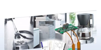
It can be used by industrial equipment, office automation equipment and home appliance manufacturers in detection systems.
The touchkey microcontrollers’ capacitive touch sensor is sensitive and has a high resistance to noise, explains Renesas. This enables the Material Detection Solution to detect the presence or absence of a powder such as vacuum cleaner dust, a liquid such as refrigerator and coffee maker, or material such as paper by measuring the capacitance between electrodes to the microcontroller. The increase or decrease of the powder, liquid, or material will change the capacitance value between the electrodes.
The development reflects the increased demand for sensor-based technology in industry, the office and the home. These applications require fine-grained sensing for predictive maintenance capabilities. The Material Detection Solution can be used to detect the remaining amounts of consumable materials in, for example vacuum cleaner filters or printers, and inform users in advance when replacements are required.
Although these applications can be implemented by using a mix of pressure sensors for detecting physical objects, photosensors, IR sensors, and CMOS sensors, the use of multiple sensors creates additional cost and heavy development burdens, points out Renesas.
The sensor-less physical object detection connects two thin-film electrodes and measures the capacitance between them using a touchkey microcontroller. Changes in the measured materials are determined by detecting the change in capacitance between the electrodes.
This method eliminates the need for sensor evaluation and operating condition determination, while the initialisation and sensitivity adjustments can be performed using the development support graphical user interface (GUI) tool available for capacitive touch sensor systems. Renesas add that this enables developers to quickly implement a capacitive touch sensor unit in equipment that require a detection function.
The Material Detection Solution is available now for free download.