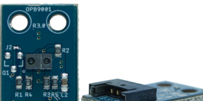
Wide-angle thermal MEMS sensor contactless offers Omron’s widest field of view

Omron Electronic Components Business Europe has added a wide angle 32 x 32 element version of its D6T MEMS thermal sensor. It offers the widest field of view that Omron has ever delivered, says the company.

The Omron D6T-32L-01A can view across 90.0 x 90.0 degrees, enabling it to encompass a wide area, such as a whole room, from a single point. The sensor offers contactless measurement of temperatures of 0 to 200 degrees C in ambient temperatures of -10 to + 70 degrees C.

Omron D6T MEMS thermal sensors are based on an IR sensor which measures the surface temperature of objects without touching them using a thermopile element that absorbs radiated energy from the target object. They incorporate a MEMS thermopile, custom designed sensor ASIC and signal processing microprocessor and algorithm in a tiny package. According to Omron, the D6T offers the highest signal-to-noise ratio (SNR) in the industry. It converts the sensor signal to a digital temperature output giving a straightforward interface to a microcontroller. The design of the D6T, which measures only 14 x 8 x 8.93mm for the largest 32 x 32 element version, makes it well-suited to temperature detection in a range of IoT and other embedded applications.

The D6T-32L is one of three D6T variants by Omron, joining the 1×8 D6T-8L-09H and the 4×4 D6T-44L-06H, offering 54.5 x 5.5 and 44.2 by 45.7 degrees respectively. These two devices offer contactless temperature measurement between 5.0 to 200 degrees C at ambient temperatures of 5.0 to 45 degrees C.

The D6T sensors can be used to detect abnormal temperatures in industrial equipment on the production line to monitoring of food and other temperatures in the kitchen. This can save costs, allowing preventative maintenance to be undertaken in a timely manner, points out Omron, and can even save lives. They can also detect the presence and location of people in a space accurately and reliably.

http://components.omron.eu  

> Read More

GigaDevice claims a first for open source RISC-V based 32-bit mcu

Believed to be the world’s first open source RISC-V based GD32V series 32-bit general purpose microcontroller (MCU), the GD32 family is announced by GigaDevice. The company says it offers tool chain support from MCU to software libraries and development boards, creating a strong RISC-V development ecosystem.

The first product line in the family is the GD32VF103 series RISC-V MCU. It is designed for mainstream development, says GigaDevice. There are 14 models, including QFN36, LQFP48, LQFP64 and LQFP100, compatible with existing GD32 MCUs in software development and pin packaging.

According to GigaDevice, the design accelerates the development cycle between GD32’s Arm core and RISC-V core products, making product selection and code porting flexible and simple. The GD32VF103 devices are specifically targeted for embedded applications ranging from industrial control, consumer electronics, IoT, edge computing to artificial intelligence and deep learning.

The GD32VF103 MCU series adopts the Bumblebee processor core based on the open source RISC-V instruction set architecture, jointly developed by GigaDevice and Nuclei System Technology. The Bumblebee core uses a 32-bit RISC-V open source instruction set architecture and supports custom instructions to optimise interrupt handling. It is equipped with a 64-bit wide real-time timer and can also generate timer interrupts defined by the RISC-V standard, with support of dozens of external interrupt sources, while possessing 16 interrupt levels and priorities, interrupt nesting and fast vector interrupts processing mechanism.

The low-power management unit can support two-levels of sleep mode. The core supports standard JTAG interfaces and RISC-V debug standards for hardware breakpoints and interactive debugging. The Bumblebee core supports the RISC-V standard compilation tool chain, as well as Linux/Windows graphical integrated development environment.

The core is designed with a two-stage variable-length pipeline microarchitecture with a streamlined dynamic branch predictor and instruction pre-fetch unit. The performance and frequency of the traditional architecture three-stage pipeline can be achieved at the cost of the two-stage pipeline, achieving industry-leading energy efficiency and cost advantages, claims GigaDevice.

The GD32VF103 MCU operates at up to 153DMIPS at the highest frequency and under the CoreMark test achieves 360 performance points. This is a 15 per cent performance improvement compared to the GD32 Cortex-M3 core. Dynamic power consumption is reduced by 50 per cent and the standby power consumption is reduced by 25 per cent, adds the company.

The GD32VF103 series RISC-V MCUs provide a processing frequency of 108MHz, 16kbyte to 128kbyte of on-chip flash and 6 to 32kbyte of SRAM cache, equipped with the gFlash patented technology, which supports high-speed core accesses to flash in zero wait time. The core also includes a single-cycle hardware multiplier, hardware divider and acceleration unit for advanced computing and data processing challenges.

The chip is powered by 2.6 to 3.6V and the I/O ports can withstand 5V voltage level. It is equipped with a 16-bit advanced timer supporting three-phase PWM complementary outputs and Hall acquisition interface for vector control. It also has up to four 16-bit general-purpose timers, two 16-bit basic timers, and two multi-channel DMA controllers. The interrupt controller (ECLIC) provides up to 68 external interrupts and can be nested with 16 programmable priority levels to enhance the real-time performance of high-performance control.

Peripheral resources include up to three USART, two UART, three SPI, two I2C, two I2S, two CAN2.0B, one USB 2.0 FS OTG and an External Bus Expansion Controller (EXMC). The I2C interface supports Fast Plus (Fm+) mode with frequencies up to 1MHz (1Mbits per second), which is two times faster than the previous speed, says GigaDevice. The SPI also supports four-wire system and more transmission modes, including the easy expansion to Quad SPI for high-speed NOR Flash accesses. The USB 2.0 FS OTG interface provides multiple modes such as device, host, and OTG, while the EXMC connects to external memory such as NOR Flash and SRAM.

The GD32VF103 series RISC-V MCUs also integrate two 12-bit high-speed ADCs with sampling rates up to 2.6Msamples per second, provides up to 16 reusable channels, supports 16-bit hardware oversampling filtering and resolution configurability and it has two 12-bit DAC. Up to 80 per cent of GPIOs have optional features and support port remapping.

http://www.gigadevice.com

> Read More

Intel ships 10nm Agilex FPGAs for networking, 5G and data analytics

Shipments have commenced for the Intel Agilex field programmable gate arrays (FPGAs). The devices are being used by early access program customers to develop advanced solutions for networking, 5G and accelerated data analytics.

Participants in the early access program include Colorado Engineering, Mantaro Networks, Microsoft and Silicom.

Dan McNamara, Intel senior vice president and general manager of the Networking and Custom Logic Group, said that the Agilex FPGA family leverages architecture, packaging, process technology, developer tools and a fast path to power reduction with eASIC technology to enable new levels of  heterogeneous computing, system integration and processor connectivity. It will be the first 10nm FPGA to provide cache-coherent and low latency connectivity to Intel Xeon processors with the upcoming Compute Express Link, he added.

The Agilex FPGAs are expected to provide the agility and flexibility that is demanded by data-centric, 5G-fuelled operations where networking throughput must increase and latency must decrease. Intel Agilex FPGAs deliver “significant gains in performance and inherent low latency,” says the company. They are reconfigurable and have reduced power consumption, together with computation and high-speed interfacing capabilities that enable smarter, higher bandwidth networks to be created. They also contribute to delivering real-time actionable insights via accelerated artificial intelligence (AI) and other analytics performed at the edge, in the cloud and throughout the network.

According to Doug Burger, technical fellow, Azure Hardware Systems at Microsoft, the software company has been working closely with Intel on the development of the Agilex FPGAs and is planning to use them in accelerating real-time AI, networking and other applications/infrastructure across Azure Cloud Services, Bing and other data centre services.

The Intel Agilex family combines second-generation HyperFlex FPGA fabric built on Intel’s 10nm process, which is up to 40 per cent higher performance or up to 40 per cent lower total power compared with Intel Stratix 10 FPGAs. There is also the heterogeneous 3D silicon-in-package (SiP) technology based on Intel’s proven embedded multi-die interconnect bridge (EMIB) technology. As a result, Intel can integrate analogue, memory, custom computing, custom I/O and Intel eASIC device tiles into a single package along with the FPGA fabric.

Intel also says they are the only FPGAs that support hardened BFLOAT16, with up to 40TFLOPS of digital signal processor (DSP) performance. They also have the ability to scale for higher bandwidth compared with PCIe Gen 4, due to the use of PCIe Gen 5.

Transceiver data rates support up to 112Gbits per second for high-speed networking requirements for 400GE and beyond. There is also support for memory option, such as current DDR4, upcoming DDR5, HBM, and Intel Optane DC persistent memory.

Design development support for Intel Agilex FPGAs is available today via Intel Quartus Prime Design Software.

http://www.intel.com

> Read More

“World’s largest chip” has more compute cores for data access

Claimed to be the largest chip in the world, the Cerebras wafer scale engine (WSE) measures 216 x 216mm (8.5 x 8.5 inch). At 46,225mm2 the chip is 56x larger than the biggest graphics processing unit (GPU) ever made, claims Cerebras.

It has 400,000 cores and 18Gbyte on-chip SRAM. The large silicon area, more than the largest graphics processing unit, enables the WSE to provide more compute cores, tightly coupled memory for efficient data access, and an extensive high bandwidth communication fabric for groups of cores to work together, claims Cerebras.

The WSE contains 400,000 sparse linear algebra (SLA) cores. Each core is flexible, programmable, and optimised for the computations that underpin most neural networks. Programmability ensures the cores can run all algorithms for constantly changing machine learning operations.

The cores on the WSE are connected via the Swarm communication fabric in a 2D mesh with 100 petabytes (Pbytes) per second of bandwidth. The Swarm on-chip communication fabric delivers breakthrough bandwidth and low latency at a fraction of the power draw of traditional techniques used to cluster GPUs, says Cerebras. It is fully configurable. Software configures all the cores on the WSE to support the precise communication required for training the user-specified model. For each neural network, Swarm provides an optimised communication path.

The 18Gbyte of on-chip memory is accessible within a single clock cycle, and provides 9 Pbytes per second memory bandwidth. This is 3,000 times more capacity and 10,000 times greater bandwidth than the leading competitor, claims Cerebras. The WSE provides moree cores, more local memory and enables fast, flexible computation, at lower latency and with less energy than other GPUs, concludes Cerebras.

https://www.cerebras.net/technology/

> Read More

About Smart Cities

This news story is brought to you by smartcitieselectronics.com, the specialist site dedicated to delivering information about what’s new in the Smart City Electronics industry, with daily news updates, new products and industry news. To stay up-to-date, register to receive our weekly newsletters and keep yourself informed on the latest technology news and new products from around the globe. Simply click this link to register here: Smart Cities Registration