World-leading out-band management for edge artificial intelligence (AI) devices, is claimed by Aetina as it unveils how it has integrated Innodisk’s InnoAge into its Jetson edge computing platform.
Management is critical in edge devices used in vertical applications, says Aetina.
It has integrated what is believed to be the industry’s first out-of-band management solid state device (SSD) InnoAge with the Aetina Jetson edge computing platform. The result reduces the cost of manually repairing the edge device and primarily reduces the downtime of the equipment, says Aetina, for convenient control of edge devices.
The integrated system effortlessly restarts and restored in the event of the edge device crashing, reports Aetina.
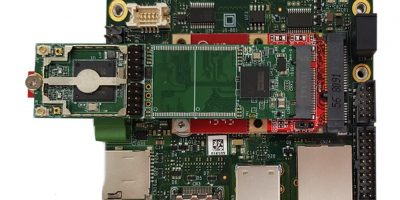
Its Jetson edge computing platform has a small form factor and low power consumption, making it suitable for embedded edge devices.
To maintain numerous edge devices, in-band management could be limited if an unpredictable issue occurs which makes it more expensive in terms of labour costs as well as possibly extending the downtime of edge devices.
InnoAge SSD equipped with an Azure Sphere chip can cut a separate space in the solid state hard disk and install a separate operating system. InnoAge connected with Azure Cloud and the system of the device can automatically be stored in the solid state hard disk. Once the operating system or software of the edge device crashes, the user can reset or restore the system of edge devices through the management platform on Azure Cloud. The real-time status of edge devices can also monitor the cloud management platform, which facilitates remote control and management of many edge devices.
Aetina says that the Azure Sphere provides the world’s premier data security ability, making the inference results of edge AI computing secure for uploading to the cloud database without security risks.
Aetina was founded in Taiwan in 2012. It provides support for general purpose graphics processing units (GPGPU) and Jetson edge AI computing solutions for embedded applications.