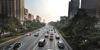
AI computing targets smart transportation and healthcare

The AN110-XNX edge AI computer developed by Aetina is based on the Nvidia Jetson Xavier NX. It is designed for applications in smart transportation, factories, retail, healthcare, AIoT and robotics.

The AN110-XNX combines the Nvidia Jetson Xavier NX and Aetina AN110 carrier board and measures just 87.4 x 68.2 x 52mm (with fan). It supports the MIPI CSI-2 interface for 1one 4k or two FHD cameras to handle intensive AI workloads from ultra-high resolution cameras to more accurate image analysis. It has 384 CUDA cores, 48 Tensor cores and cloud-native capability to deliver up to 21 Terra operations per second (TOPS).

Bundled with the latest Nvidia Jetpack 4.4 software development kit (SDK), the AN110-NX is an energy-efficient module for embedded edge-computing performance capabilities to support AI workloads which may be constrained by size, weight, power budget, or cost.

Aetina offers a full system, AN110-XNX-EN70 with fanless chassis and back up support in the form of board support packages and design to build configuration updates for both standard and customised platforms in their service policy. Aetina is developing Jetson Xavier NX-based edge computing platforms with 5G communications capability and full function browser-based edge device management.

As an Nvidia-preferred partner, Aetina focuses on delivering edge AI computing based on the Jetson platform for embedded applications. Nvidia Jetson is the leading AI-at-the-edge computing platform, with nearly half a million developers, says Aetina. Support for cloud-native technologies is now available across the Nvidia Jetson lineup, for manufacturers of intelligent machines and developers of AI applications to build and deploy software-defined features on embedded and edge devices targeting robotics, smart cities, healthcare and the industrial IoT.

The AN110-XNX is available now.

Aetina was founded in Taiwan in 2012 as a provider of high-performance general purpose graphics processor unit (GPGPU) and edge AI computing based on the Nvidia Jetson platform for embedded applications. We provide industrial components, system integration and services focused on the industrial and AIoT markets.

http://www.aetina.com

> Read More

Automotive wafer-level camera module monitors more vehicles

Believed to be the industry’s first automotive-grade, wafer-level camera, the OVM9284 CameraCubeChip module is an automotive-grade, wafer-level camera, developed by OmniVision Technologies. The one Mpixel module is compact, measuring 6.5 x 6.5mm, enabling it to be placed in more places with the cabin as part of the vehicle’s driver monitoring system (DMS), while being hidden from view. It is also claimed to be the lowest power consumption among automotive camera modules—over 50 per cent lower than the nearest competitor. This enables it to run continuously in the tightest of spaces and at the lowest possible temperatures for maximum image quality.

The OVM9284 is built on OmniVision’s OmniPixel 3-GS global-shutter pixel architecture, which is claimed to provide quantum efficiency at the 940nm wavelength for the highest quality driver images in near or total darkness. The integrated OmniVision image sensor has a three micron pixel and a 0.25 inch optical format, along with 1280 x 800 resolution.

“The accelerated market drive for DMS is expected to generate a 43 per cent CAGR between 2019 and 2025, said Pierre Cambou, principal analyst, imaging at Yole Développement. “DMS is probably the next growth story for ADAS cameras as driver distraction is becoming a major issue and has brought regulator attention,” he added.

“Most existing DMS cameras use glass lenses, which are large and difficult to hide from drivers to avoid distraction, and are too expensive for most car models,” said Aaron Chiang, marketing director at OmniVision. The OVM9284 CameraCubeChip module is designed to provide wafer level optics in a small, low power consumption and reflowable form factor.

The OVM9284’s integration of OmniVision’s image sensor, signal processor and wafer-level optics in a single compact package eliminates the complexity of multiple vendors and increases supply reliability while speeding development time, says the company. The CameraCubeChip modules, unlike traditional cameras, are reflowable. This means they can be mounted to a PCB simultaneously with other components using automated surface-mount assembly equipment to reduce assembly costs.

OVM9284 module samples are available now, and mass production is expected in Q4 of 2020.

OmniVision Technologies develops digital imaging and its award-winning CMOS imaging technology is claimed to enable superior image quality in many of today’s consumer and commercial applications, including mobile phones, security and surveillance, automotive, tablets, notebooks, webcams and entertainment devices, medical and AR, VR, drones and robotics imaging systems.

http://www.ovt.com

> Read More

Renesas adds to control plane options with I3C bus extension products

I3C multiplexers and I/O expanders from Renesas Electronics deliver 12.5MHz in a small footprint, claims the company.

There are four new I3C Basic bus extension products for control plane designs for data centre and server applications, as well as enterprise, factory automation and communications equipment. The IMX3102 2:1 bus multiplexer, IMX3112 1:2 bus expander, and IXP3114 and IXP3104 1:4 general-purpose I/O expanders support up to 12.5MHz speeds as well as integrated thermal sensor capability.

Engineers can use them when implementing I3C Basic as a system management bus in applications where there may be multiple masters, a large number of endpoint devices and long traces affecting bus complexity and signal integrity. The integrated thermal sensor allows the thermal management to be integrated into the bus design itself and can reduce the number of dedicated thermal sensor endpoints.

According to Renesas, next-gen compute architectures are leading the transition to I3C as the system management bus of choice, as a result of the JEDEC standard’s adoption of I3C Basic for the DDR5 memory sideband. The increase in memory subsystem complexity with distributed power management, telemetry and thermal management at the sub-channel level requires higher sideband bus bandwidth, observes the company.

Demand for advanced thermal control loops, security and component authentication, and more robust fault tolerance and recovery are driving the need for a high bandwidth interface across the entire server control plane. I3C Basic enables system management architectures to provide granular information about the server resource status during boot-up and runtime. This allows system managers to implement effective workload migration and server load balancing to “significantly optimise” server utilisation.

The IMX3102 2:1 bus multiplexer is suitable for designs where there may be two masters controlling a single peripheral or slave devices. The IMX3112 1:2 bus multiplexer supports designs where a single host is controlling two peripheral or slave devices. The general-purpose I/O expanders, IXP3114 (with temperature sensor) and IXP3104 1:4 (without temperature sensor), are designed for a host controller with up to four peripheral or slave devices.

The new I3C products feature integrated temperature sensors. Unexpected motherboard temperature increases can result in costly system failures. Positioning temperature sensors in multiple locations on the motherboard allows engineers to continuously monitor for potential temperature spikes and direct the CPU to take action to prevent a catastrophic event.

Additional features include a two-wire programmable I2C or I3C Basic bus serial interface, a single device load on the host bus and single 1.8V input power supply. The integrated temperature sensor accuracy is 0.5 degrees C with 0.25 degrees C resolution and the industrial operating temperature range is -40 to +125 degrees C.

The devices are supplied in a thermally enhanced, nine-pin PSON-8 package, measuring 2.0 x 3.0mm.

The I3C devices and evaluation boards are sampling now to qualified customers.

http://www.renesas.com

> Read More

Green Hills Software introduces software development tools for RISC-V 

Software development tools targeting 32- and 64-bit RISC-V processor architectures have been announced by Green Hills Software. The company announced availability and early customer adoption of its Multi integrated development environment (IDE), multi-core debugger, optimising C/C++ compilers and hardware JTAG probe for software developers targeting pre-silicon and silicon platforms using RISC-V.

The tools for RISC-V can help developers achieve shorter development times, higher processor performance, and to gain competitive differentiation through the RISC-V’s custom instructions and modular instruction set architecture, says Green Hills.

The Green Hills software development tools support both 32-bit and 64-bit RISC-V architectures and provide for the integer, multiply/divide, atomic, compressed, and single- and double-precision floating point modules. Users can add their own custom RISC-V instructions for use in the Green Hills’ compiler, assembler, Multi debugger, and instruction set simulator. RISC-V’s separate privileged instruction set specification is also supported.

Green Hills compilers support ISO/IEC 14882:2011 (C++11), ISO/IEC 14882:2014 (C++14) and ISO/IEC 14882:2017 (C++17) which offers a number of new language features and standard libraries. They also support Embedded C++ and GNU C/C++ extensions.

Certification support and evidence for MULTI and the C/C++ run-time libraries for RISC-V will be available in CY2021 to enable customers’ FuSa production program requirements.

To help prevent new software bugs in RISC-V applications, an integrated MISRA C/C++ Adherence Checker for MISRA 2004 and MISRA 2012 is seamlessly integrated in the Multi development tools and the DoubleCheck static source analyser identifies programming errors. DoubleCheck automatically runs during compilation, differentiating it from traditional static analysis tools which run separately from the compiler. The Run Time Error Checking tool complements DoubleCheck by finding bugs at run-time that cannot be identified by static analysis alone.

The Multi development tools can quickly identify and solve problems during software development on RISC-V and other 32- and 64-bit processor architectures. They include the Multi debugger and JTAG probe for single-window debugging and control on complex heterogenous SoCs comprised of one or more RISC-V cores with other cores.

The Profiler pinpoints performance bottlenecks by clearly displaying processor times consumed by each task, function, source line, and assembly language instruction.

The Multi development tools, optimizing C/C++ compilers and Green Hills Probe for RISC-V are available today.

https://ghs.com/go/risc-v

> Read More

About Smart Cities

This news story is brought to you by smartcitieselectronics.com, the specialist site dedicated to delivering information about what’s new in the Smart City Electronics industry, with daily news updates, new products and industry news. To stay up-to-date, register to receive our weekly newsletters and keep yourself informed on the latest technology news and new products from around the globe. Simply click this link to register here: Smart Cities Registration