Max-M12 connector supports high-speed transmission in harsh environments

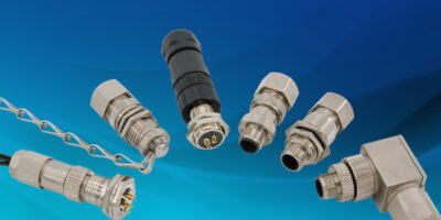
Amphenol Industrial Operations has enhanced its Max-M12 product line to include an X coding, high-speed connector with support for 10Gbits per second (1000M Ethernet with CAT6 cable) data transmission and S coding for a safer connection with ‘first mate last break’. The connectors are for use in the rail and mass transit (RMT), heavy equipment vehicles, industrial automation and robotics markets.

When used on RMT door systems, on camera and communication systems, as well as on heating, ventilation, air conditioning (HVAC) systems, the Max-M12 can transmit high speed data in environments where there is high vibration, moisture, salt, dirt and debris. It can also be used for off-road vehicles, ruggedised factory automation and robotics signal applications.

The Max-M12 family of connectors is based on IEC 61076-2-101 and SAE J2839. They are backwards-compatible and can be mated with any standard M12 connector with the same indexing, assures Amphenol. The Max-M12 features several mounting options, including front or back lock/flange and wire termination styles, including solder, crimp and printed circuit tails.

The Max-M12 is rated to 4.0A and can endure extreme temperatures ranging from -55 to +125 degrees C.

All Max-M12 connectors have an IP67 rating making them dust and waterproof. They are resistant to high pressure wash downs and water immersion.  Amphenol has plating designed to endure salt spray testing for up to 240 hours for use in harsh environments.

Amphenol’s Max-M12 connector in-line mated pair can withstand 444N of connector-to-cable retention forces and contact retention forces to 110N. Housed in an HDM 12 EX impact resistant metal or plastic shell, the in-line mated pair is available as a 90 degrees right angle or straight versions. When shielding is required the Max-M12 metal version is available in multiple shell styles for a variety of interconnect requirements.  Both the four- and five-pin configurations are available with A, B and D polarity codes.

Amphenol Industrial Operations is headquartered in Endicott, New York, USA, providing a range of high reliability power/signal connectors and interconnection systems specifically for the industrial markets including rail/mass transit, process control, automotive manufacturing, heavy equipment, wireless base stations and petrochemical/power generation.

Its product range includes ruggedised-for-industry cylindrical, fibre optic, rectangular, and industrialised versions of Amphenol’s MIL-DTL-5015 cylindrical, MIL-DTL-26482 miniature cylindrical and GT reverse bayonet cylindrical connectors. It is ISO9001, TS96949 and MIL-STD-790-certified.

Amphenol Industrial Operations is a division of Amphenol, one of the largest manufacturers of interconnect products in the world.

http://www.amphenol-industrial.com

> Read More

Open source software stack eases security integration, says Infineon

Trusted Platform Modules (TPM) enable secured remote software updates, disc encryption and user authentication in connected embedded devices in industrial and automotive applications. Infineon provides its Optiga TPM 2.0 software stack to facilitate seamless integration in Linux-based systems. The TPM software stack implements the latest feature application programming interface (FAPI) standard. Infineon has developed the open-source software jointly with Intel Corporation and Fraunhofer Institute for Secure Information Technology (SIT).

According to Infineon, using the Optiga TPM 2.0 allows IoT system integrators to “significantly improve” the security of connected products. Software integration with TPM software stack (TSS) -FAPI does not require specific skills in low-level security specifications and reduces source code development by a factor of up to 16, claims Infineon. This can result in reduced time to market as manufacturers can accelerate the process for certifying industrial devices according to the IEC 62443 standard for industrial applications, which requires hardware-based safety from level 4 upwards.

The FAPI specification was released as an international standard by the Trusted Computing Group (TCG). The specification is implemented in the TSS stack 1 with the associated tools and plug-ins. The TSS stack is open source software, which allows seamless integration of the TPM 2.0 in Linux-based systems. This includes the support of typical Linux software for device authentication, data encryption, software updates and remote device management.

The FAPI enables the native support of the PKCS#11 standard as a generic interface for user authentication, single sign-on and email encryption/signing. The FAPI provides a default configuration for cryptographic functionalities, system integration and automated processing of security mechanisms, says Infineon.

The Optiga TPM acts as a vault for sensitive data in connected devices and lowers the risk of data and production losses due to cyber attacks. Infineon’s TPMs are certified by independent certification bodies according to the Common Criteria, an international set of guidelines and specifications developed for evaluating information security products. The TSS stack including the recent FAPI has been verified to achieve compliance and interoperability.

Application developers can use the Optiga TPM SLB 9670, Optiga TPM SLI 9670 and Optiga TPM SLM 9670 Iridium boards and TSS Quickstarter now. There are also board and source code packages for the Infineon Aurix and for the Arduino microcontrollers.

http://www.infineon.com

> Read More

First IP for PCI Express 6.0 has low latency for HPC and AI

IP that supports the latest features in the PCI Express (PCIe) 6.0 specification has been released by Synopsys. The DesignWare IP can be used for early SoC development, high performance computing and artificial intelligence (AI).

The IP for PCIe 6.0 includes controller, PHY and verification IP, for early development of PCIe 6.0 SoCs. It supports the latest features in the standard specification including, 64 GT/s PAM-4 signalling, FLIT mode and L0p power state. Acccording to Synopsys the IP addresses evolving latency, bandwidth and power-efficiency requirements of high performance computing (HPC), AI and storage SoCs.

To achieve the lowest latency with maximum throughput for all transfer sizes, the DesignWare Controller for PCI Express 6.0 uses a MultiStream architecture, delivering up to x2 the performance of a single-stream design. The controller, with available 1024bit architecture, allows designers to achieve 64Gtransfers per second x16 bandwidth and closing timing of 1GHz. The controller provides optimal flow with multiple data sources and in multi-virtual channel implementations. To facilitate accelerated testbench development with built-in verification plan, sequences and functional coverage, the VC Verification IP for PCIe uses native SystemVerilog/UVM architecture that can be integrated, configured and customised.

Synopsys’ DesignWare PHY IP for PCIe 6.0 provides adaptive DSP algorithms that optimise analogue and digital equalisation to maximise power efficiency regardless of the channel. The PHY enables near zero link downtime using patent-pending diagnostic features. The placement-aware architecture of the DesignWare PHY IP for PCIe 6.0 minimises package crosstalk and allows dense SoC integration for x16 links, added Synopsys. The datapath is optimised with ADC-based architecture for low latency.

The DesignWare Controller and PHY IP for PCIe 6.0 early access are scheduled to be available in Q3 of 2021. The Verification IP for PCIe 6.0 is available now.

Synopsys develops silicon-proven IP for SoC designs. The DesignWare IP portfolio includes logic libraries, embedded memories, PVT sensors, embedded test, analogue IP, wired and wireless interface IP, security IP, embedded processors and sub-systems. Synopsys’ IP Accelerated initiative offers IP prototyping kits, IP software development kits and IP subsystems accelerate prototyping, software development and integration of IP into SoCs. The company’s invests in IP quality, comprehensive technical support and robust IP development methodology to enable designers to reduce integration risk and accelerate time-to-market.

Image credit- iStock,DKosig

https://www.synopsys.com

> Read More

Microchip introduces software-based redundancy to network timing

With the introduction of the TimeProvider 4100 release 2.2 Grandmaster, Microchip provides a new level of software-based redundancy for the IEEE 1588 precise timing grandmaster with gateway clock.

It is intended for critical infrastructure providers, e.g. 5G wireless networks, smart grids, data centres, cable and transportation services, which require redundant, resilient and secure precise timing and synchronisation solution, explained Microchip.

In addition to the redundancy architecture, the TimeProvider 4100 Release 2.2 grandmaster has support for a multi-band global navigation satellite system (GNSS) receiver and enhanced security to ensure always-on precise timing and synchronisation.

Redundancy ensures uninterrupted services. Infrastructure deployments previously relied on hardware redundancy to avoid service disruption but the modular architectures are expensive. The TimeProvider 4100 Release 2.2 grandmaster provides redundancy via software implementation, enabling flexible deployment and lower hardware costs without sacrificing ports, pointed out Microchip.

It also introduces an increased level of resiliency by supporting a new GNSS multi-band, multi-constellation receiver to protect against time delay resulting from space weather, solar events and other disruptions that may impact critical infrastructure services. Multi-band GNSS is particularly important for the highest levels of accuracy including primary reference time clock Class B (PRTC-B) (40 nano seconds) and enhanced primary reference time clock (ePRTC) (30 nano seconds).

The TimeProvider 4100 Release 2.2 grandmaster also adds support for Radius and TACACS+ and also introduces anti-jamming and anti-spoofing capabilities.

In addition, the TimeProvider 4100 Release 2.2 grandmaster provides a super oven controlled crystal oscillator (OCXO) option for enhanced holdover capabilities in case of GNSS disruption.

The TimeProvider 4100 Release 2.2 grandmaster is a family of products with hardware expansion modules for legacy fan-out or Ethernet fan-out with 10Gigabit Ethernet support. It can be configured in specific operation modes to act either as a gateway clock, a high-performance boundary clock or an ePRTC.

The TimeProvider 4100 Release 2.2 grandmaster embeds additional Microchip technology including its OCXO, super OCXO, Rubidium atomic clock, field programmable gate arrays (FPGAs), Ethernet switch, synthesisers and cleaning oscillators.

The TimeProvider 4100 is part of Microchip’s virtual Primary Reference Time Clock (vPRTC) product portfolio, offering end-to-end precise time and synchronisation. The portfolio also includes Cesium atomic clocks for source of frequency and time, the BlueSky GNSS firewall for security, TimeProvider 4100 high-performance boundary clock and TimeProvider 4100 gateway clocks, as well as the TimePictra software suite, which manages the end-to-end precise time architecture across all Microchip timing products.

Microchip’s TimeProvider 4100 Release 2.2 grandmaster offers several options for software and hardware support including installation, sync audits, network engineering and 24/7 worldwide support.

The TimeProvider 4100 Release 2.2 grandmaster is available now for both new and already-deployed systems.

http://www.microchip.com

> Read More

About Smart Cities

This news story is brought to you by smartcitieselectronics.com, the specialist site dedicated to delivering information about what’s new in the Smart City Electronics industry, with daily news updates, new products and industry news. To stay up-to-date, register to receive our weekly newsletters and keep yourself informed on the latest technology news and new products from around the globe. Simply click this link to register here: Smart Cities Registration