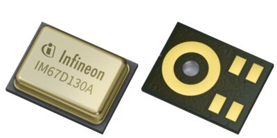
Arm announced first new architecture in a decade

In response to demand for specialised processing, security and artificial intelligence (AI), Arm has introduced the Armv9 architecture.

At the launch, CEO Simon Segars said “As we look toward a future that will be defined by AI, we must lay a foundation of leading-edge compute that will be ready to address the unique challenges to come”.

The new capabilities in Armv9 will accelerate the move from general-purpose to more specialised compute across every application as AI, the IoT and 5G gain momentum internationally.

To secure data, the Armv9 roadmap introduces the Arm Confidential Compute Architecture (CCA). Confidential computing shields portions of code and data from access or modification while in-use, even from privileged software, by performing computation in a hardware-based secure environment.

The Arm CCA will introduce the concept of dynamically created realms, useable by all applications, in a region that is separate from both the secure and non-secure worlds. For example, in business applications, realms can protect commercially sensitive data and code from the rest of the system while it is in-use, at rest, and in transit. Availability of confidential computing could bring down the cost of security, reports Arm.

The ArmV9 confidential compute features were developed in collaboration with Microsoft.  “The increasing complexity of use cases from edge to cloud cannot be addressed with a one-size-fits-all solution,” said Henry Sanders, corporate vice president and chief technology officer, Azure Edge and Platforms at Microsoft. “As a result, heterogeneous compute is becoming more ubiquitous, requiring greater synergy among hardware and software developers.”

The range of AI workloads demands more diverse and specialised solutions, with AI-enable voice assistance as one example.

Arm partnered with Fujitsu to create the Scalable Vector Extension (SVE) technology, which is at the heart of Fugaku, the world’s fastest supercomputer. Arm has developed SVE2 for Armv9 to enable enhanced machine learning (ML) and digital signal processing (DSP) capabilities across a wider range of applications.

SVE2 enhances the processing ability of 5G systems, virtual reality and augmented reality (VR and AR) and ML workloads running locally on CPUs, such as image processing and smart home applications. Arm says it will extend the AI capabilities of its technology with “substantial enhancements” in matrix multiplication within the CPU, in addition to ongoing AI innovations in Mali GPUs and Ethos NPUs.

Armv9 CPUs are expected to increase by more than 30 per cent over the next two generations of mobile and infrastructure CPUs.

To meet the demands of ubiquitous specialised processing, Arm’s Total compute design methodology, together with enhanced specialised processing, will accelerate overall compute performance through focused system-level hardware and software optimisations and increases in use-case performance, says Arm.

Arm will apply Total Compute design principles across the automotive, client, infrastructure and IoT IP portfolios. It is also developing several technologies to increase frequency, bandwidth, and cache size, and reduce memory latency, adds the company.

A unique vision for the next decade of computing

Richard Grisenthwaite, senior vice president, chief architect and fellow at Arm, believes: “Armv9 will enable developers to build and program the trusted compute platforms of tomorrow by bridging critical gaps between hardware and software, while enabling the standardization to help our partners balance faster time-to-market and cost control alongside the ability to create their own unique solutions.”

http://www.arm.com

> Read More

Renesas concentrates on communications for RA6 series microcontroller additions

The RA6M5 group of microcontrollers completes Renesas Electronics’ RA6 series Arm Cortex M33-based devices. The company has added 20 microcontrollers to complete the RA6 series. The RA6M5 group of microcontrollers offer communications options, generous on-chip memory, and what Renesas claims to be best-in-class security features.

Communications interface options include CAN FD, Ethernet MAC with DMA, USB full speed and high speed, and multiple serial interfaces. Renesas claims that designers of IoT systems will have “unmatched flexibility” in sharing critical data using the RA6M5 Group.

The new microcontrollers integrate up to 2Mbyte of on-chip flash and 512kbyte on-chip RAM. They also provide an OctaSPI which enables designers to extend the on-chip flash and RAM. The microcontrollers also support error correction code (ECC) in the RAM.

The memory block swap feature and intrinsic security in the RA devices are claimed to make the RA6M5 group particularly suitable for in-field firmware update applications. After new firmware is written to the flash using background operation, a selectable amount of 32kbyte flash blocks can be swapped to the new firmware.

The RA6M5 microcontrollers have an Arm Cortex-M33 core based on Armv8-M architecture. They feature Arm TrustZone technology and Renesas’ secure crypto engine. The engine incorporates multiple symmetric and asymmetric cryptography accelerators, advanced key management, security lifecycle management, power analysis resistance, and tamper detection.

They are also characterised by very Low power consumption of 107 microA/MHz in active mode (running the CoreMark algorithm from flash at 200MHz) and 30 microseconds wake up time.

The microcontrollers are scalable from 100- to 176-pin LQFP packages and also available in 176-ball BGAs.

The RA6M5 group is supported by the Flexible Software Package (FSP), which includes a best-in-class HAL driver, says Renesas. The FSP uses a graphical user interface (GUI) to simplify and accelerate the development process, while also making it easy for customers to transition from an original 8/16-bit microcontroller design. Designers using the RA6M5 microcontrollers also have access to the extensive Arm partner ecosystem, offering a wide range of tools that help speed time-to-market.

The RA6M5 microcontrollers and the EK-RA6M5 evaluation kit (RTK7EKA6M5S00001BE) are available now from Renesas and its worldwide distributors.

http://www.renesas.com

> Read More

Anritsu and MediaTek achieve FR1+FR2 dual connectivity for 5G rollout

Achieving what is claimed to be an industry first, Anritsu announces that its radio communication test station MT8000A has achieved a downlink throughput over 7Gbits per second using FR1+FR2 dual connectivity and 256QAM in 5G standalone mode in conjunction with MediaTek’s M80 5G modem. This increased data throughput is cited as a key factor in facilitating mobile services and new services for 5G.

FR1+FR2 DC combines FR1 and FR2 technologies to improve data throughput per user by grouping cell base stations with different frequency ranges to transmit data. The 256QAM technology uses RF and signal processing technologies to support faster communications by sending 8-bits of data in a single symbol.

The combination of FR1+FR2 DC technology with 256QAM supporting downlink throughput speeds greater than 7Gbits per second represents an important milestone in future growth of 5G services, says Anritsu.

The radio communication test station MT8000A supports RF and protocol testing, functional and application operation testing and beam characteristics testing. In addition to supporting both NSA and SA-mode base station simulation functions required for development of 5G chipsets and terminals, it also covers FR1 frequency bands, including 600MHz, 2.5, 3.5, 4.5 and 6.0GHz unlicensed bands, as well as the FR2 24, 28, 39 and 43GHz mmWave bands, to support all the main bands used by 5G services.

It also supports the functions required for high-speed communications, such as 4 x 4 MIMO in FR1, 8CC and 256QAM in FR2 and the latest 3GPP Release 16 features. The MT8000A can be configured using a simple user interface and software to test device performance.

MediaTek is a global fabless semiconductor company that enables nearly 2bn connected devices a year. It develops SoCs for mobile device, home entertainment, connectivity and IoT products for mobile technologies, automotive solutions and a broad range of advanced multimedia products such as smartphones, tablets, digital televisions, 5G, voice assistant devices (VAD) and wearables.

Anritsu provides communications test and measurement products and engages customers to help develop wireless, optical, microwave/RF, and digital solutions for R&D, manufacturing, installation, and maintenance applications, as well as multi-dimensional service assurance solutions for network monitoring and optimisation. Anritsu also provides precision microwave/RF components, optical devices, and high-speed electrical devices for communication products and systems. The company develops advanced solutions for 5G, M2M, IoT, as well as other emerging and legacy wireline and wireless communication markets.

http://www.anritsu.com

> Read More

Renesas combines pre-regulator and PMIC for ADAS camera systems

A 42V synchronous buck pre-regulator is combines with a seven-channel power management IC (PMIC) in a power and functional safety solution for systems based on the R-Car V3H SoC for advanced driver assistance systems (ADAS) automotive front cameras and driver monitor cameras.

Renesas has combined the RAA271050 42V synchronous buck pre-regulator that accepts the vehicle’s 12V supply and steps it down to an intermediate supply voltage of 3.3 or 5.0V. The seven channel power RAA271000 PMIC takes the RAA271050’s output and steps it down further to the various supply voltages needed by R-Car V3H and its peripherals such as LPDDR4 memory.

Both devices were developed per the ISO-26262 standard, and can support system safety requirements up to ASIL D. The solution satisfies all the power and functional safety requirements for the R-Car V3H, says Renesas. It provides supply voltages with the current capability to meet all power specifications, including sequence, voltage accuracy, and load step response. It also provides all the necessary power and digital monitoring functions.

According to Renesas the combination provides best-in-class efficiency, with power loss reductions of up to 33 per cent compared to competitive PMICs under comparable operating conditions. Lower power loss enables operation at higher temperatures, reduces cooling costs and improves reliability. The RAA271050 and RAA271000 were designed to match R-Car requirements with no unnecessary overhead, reducing both component cost and PCB area. Reference hardware includes the new components, speeding design time and reducing testing requirements for customers.

The R-CAR V solution includes programmable output voltage, sequencing, I/O configuration and safety configuration. The integrated 12-bit SAR ADC has up to 16 external inputs monitors internal and external signals, eliminating the need for an added system ADC.

Dynamic voltage frequency scaling (DVFS) adjusts output voltage to minimise power consumption and there is optional spread spectrum clocking which mitigates EMI. Support for R-Car V3H SoC activation streamlines the SoC self-test procedures, adds Renesas.

The RAA271050 and RAA271000 are included in an ADAS front camera solution featuring the EagleCam camera module from Lupa-Electronics and Renesas’ R-Car V3H and R-Car V3M SoCs.

The RAA271050 is offered in a 22-lead, 4.0 x 4.0mm QFN package. The RAA271000 is packaged in a 60-ball FCBGA with 0.8mm pitch. Both devices are sampling today and are expected to be fully available in July 2021.

http://www.renesas.com

> Read More

About Smart Cities

This news story is brought to you by smartcitieselectronics.com, the specialist site dedicated to delivering information about what’s new in the Smart City Electronics industry, with daily news updates, new products and industry news. To stay up-to-date, register to receive our weekly newsletters and keep yourself informed on the latest technology news and new products from around the globe. Simply click this link to register here: Smart Cities Registration