
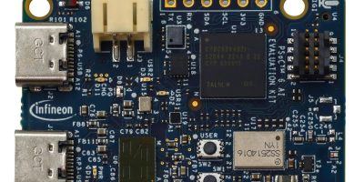
Infineon has announced the release of a comprehensive evaluation kit for embedded, Edge AI and Machine Learning (ML) system designs. The new PSoC 6 AI Evaluation Kit provides all the tools required to build intelligent consumer, smart home and IoT applications. The solution executes inferencing next to the sensor data source, providing such user benefits as enhanced real-time performance and power efficiency compared to cloud-centric solution architectures. Its small 35 mm x 45 mm form factor, affordable cost and broad range of integrated sensors and connectivity make it the perfect choice for in-field data collection, rapid prototyping, model evaluation and solution creation.
The PSoC 6 AI Evaluation Kit also leverages Infineon’s advanced microcontroller (MCU), sensor and connectivity portfolios and powerful software development environments, including the Infineon ModusToolbox and the company’s Imagimob Studio offering for custom ML models, as well as off-the-shelf Ready Models.
“Infineon is helping drive the evolution of Edge AI, which requires the real-time compute capability and power-efficiency that distinguish our hardware portfolio, along with development tools that simplify and speed application development,” said Steve Tateosian, SVP of IoT, industrial and consumer microcontrollers, Infineon Technologies. “With our newest evaluation kit, we are offering access to a complete, easy-to-use ecosystem of Infineon hardware and software that will accelerate development and deployment of intelligent solutions in consumer, smart home, commercial and industrial IoT applications.”
IoT
Click Shield from Mikroe simplifies integration of Arduino Portenta
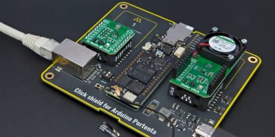
Mikroe, has announced Click shield for Arduino Portenta, a simple means of combining Arduino Portenta‘s functionality with the breadth and depth of Mikroe’s 1600+-strong family of Click board peripheral add-on boards. The shield comes equipped with two mikroBUS sockets, enabling developers to integrate a wide range of functions – from sensors and communication modules to advanced audio processing and motor control – with the powerful Arduino Portenta.
The Arduino Portenta supports simultaneous execution of Arduino code and MicroPython, offering robust connectivity options like WiFi, BLE, and optional LoRa or cellular modules. Its modular design enhances its adaptability for additional hardware, suiting it for industrial use in demanding environments such as machinery, PLCs, and robotics. Additionally, Portenta can handle AI and machine learning applications, allowing for the implementation of intelligent IoT solutions directly on the device.
The Click Shield includes several essential features to enhance the board’s functionality and ease of use. The Boot mode switch (BT SEL switch) allows users to configure the boot mode of the board, and a JTAG connector facilitates easy debugging and low-level debugging tasks or special firmware updates using an external programmer. The shield’s I2S pins are ideal for high-quality audio processing and streaming tasks on the Arduino Portenta, providing a valuable addition for developers exploring advanced multimedia projects.
Click Shield for Portenta has three vital connectors that significantly expand the board’s capabilities. The Ethernet connector enables the Portenta to connect to the internet via an Ethernet cable, allowing for robust network interactions such as sending HTTP methods or communicating with other devices and APIs. Additionally, the Shield includes a camera connector that allows the rapid development of machine vision applications. This enables the Portenta to transform into an industrial camera capable of performing real-time machine-learning algorithms on live video feeds. Thanks to the MicroSD card holder on the Click Shield, captured frames can be encoded to bitmap standards and saved to an SD Card, and configuration files can also be read from the SD card, enhancing the board’s utility in complex projects.
ST releases 750W motor-drive reference board in tiny outline
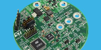
The EVLDRIVE101-HPD (High Power Density) motor-drive reference design by ST packs a 3-phase gate driver, STM32G0 microcontroller, and 750W power stage on a circular PCB just 50mm in diameter. The board features extremely low power consumption in sleep mode, below 1uA, and its tiny outline can fit directly in equipment like hairdryers, handheld vacuums, power tools, and fans. It also fits easily into drones, robots, and drives for industrial equipment such as pumps and process-automation systems.
Built with ST’s STDRIVE101 3-phase gate driver, the reference design gives flexibility to choose the motor-control strategy, such as trapezoidal or field-oriented control (FOC), with sensored or sensorless rotor-position detection. The STDRIVE101 IC contains three-half bridges with 600 mA source/sink capability and operates from 5.5V to 75V to handle any low-voltage application. The chip integrates voltage regulation for the high-side and low-side gate drivers and configurable drain-source-voltage (Vds) monitoring protection. It also provides an external pin for choosing direct high-side and low-side gate inputs or PWM control.
Developers can take advantage of the STM32G0 single-wire debug (SWD) interface to interact with the microcontroller, while support for direct firmware update allows applying bug fixes and new features.
The power stage of the EVLDRIVE101-HPD reference design features STL220N6F7 60V STripFET F7 MOSFETs, which preserve efficiency with their 1,2mΩ typical Rds(on), easing plug-and-play connection of the motor. Additional features include fast-acting power-on circuitry that disconnects the power source when idle to save energy and extend operation in battery-powered applications. Protection built into the driver IC ensures system safety and efficiency, including the Vds monitoring of the power-stage MOSFETs, as well as under-voltage lockout (UVLO), overtemperature protection, and cross-conduction prevention.
New Reality AI Explorer Tier from Renesas

Renesas Electronics Corporation has introduced Reality AI Explorer Tier, a free version of the Reality AI Tools software for developing AI and TinyML solutions in industrial, automotive and commercial applications.
The new Reality AI Explorer Tier provides users with free access to a comprehensive, self-guided evaluation sandbox. Qualified customers can now access the complete range of features in Reality AI Tools, including automated AI model construction, validation and deployment modules. Reality AI Explorer Tier includes a rich library of tutorials, application examples, and FAQs, access to the community forum and email support. Users can quickly get started with a simplified click-through end user agreement.
Reality AI Explorer Tier is designed to simplify the customer experience for evaluating the development environment for embedded real-time analytics. Users can explore a variety of pre-built AI applications, offering a practical way to experience the capabilities of Reality AI Tools without the need for extensive setup or support. Examples allow the user to leverage Renesas Kits such as AI Kits with sample datasets that span use cases across accelerometry/vibration analysis, audio classification, and motor control.
“As AIoT becomes increasingly important, many customers are showing keen interest and developing expertise in building AI applications at the edge and endpoint,” said Mohammed Dogar, Vice President and Head of Business Development and Ecosystem for Renesas. “Reality AI Explorer offers the opportunity to experience the full potential of a market-leading AI development environment without any up-front cost. We are confident that many customers will use this platform as a first step to creating production AIoT implementations.”
Reality AI Tools is now tightly integrated with Renesas compute products and supports all Renesas MCUs and MPUs natively with a built-in parts picker engine. Support for automatic context switching between Reality AI Tools and e2 studio is also in place.
About Smart Cities
This news story is brought to you by smartcitieselectronics.com, the specialist site dedicated to delivering information about what’s new in the Smart City Electronics industry, with daily news updates, new products and industry news. To stay up-to-date, register to receive our weekly newsletters and keep yourself informed on the latest technology news and new products from around the globe. Simply click this link to register here: Smart Cities Registration

