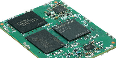
Face recognition uses 3D SLM camera and NXP’s i.MX RT117F crossover MCU 

A 3D face recognition access control systems uses  NXP Semiconductor’s crossover MCU with a 3D camera to enable faster secure face recognition under challenging lighting conditions.

The 3D structured light module (SLM) camera is combined with the i.MX RT117F crossover MCU and is believed to be the first time a 3D SLM camera has been combined with an MCU to deliver the performance and security of 3D face recognition at the edge. It therefore removes the need to use an expensive and power-hungry Linux implementation on a microprocessor which is conventionally the case with high-performance 3D cameras, reports NXP.

The i.MX RT117F MCU is part of the i.MX RT1170 family of crossover MCUs. It is based on an Arm Cortex-M7 CPU with 2Mbyte of on-chip SRAM, running at up to 1GHz. 

The turnkey system is the latest EdgeReady solution from NXP. It enables developers of smart locks and other access control systems to add machine learning-based secure face recognition quickly and easily to smart home and smart building products. Reliable 3D face recognition can be achieved in indoor and outdoor applications, across varied lighting conditions, including bright sunlight, dim night light, or other difficult lighting conditions that are challenging for traditional face recognition systems.

The use of a 3D SLM camera enables advanced liveness detection, helping distinguish a real person from spoofing techniques, such as a photograph, imitator mask or a 3D model, to prevent unauthorised access.

The i.MX RT117F uses an advanced machine learning model as part of NXP’s eIQ machine learning software running on its CPU core.

 Advanced liveness detection and face recognition are performed locally at the edge, making it possible for personal biometric data to remain on the device. This helps address consumer privacy concerns, while also eliminating the latency associated with cloud-based solutions.

The development kit for this 3D face recognition system, the SLN-VIZN3D-IOT, will be available later in November from NXP and authorised distributors.

The i.MX RT117F includes a license to use the NXP 3D face recognition software development kit (SDK), and is available in consumer, industrial and automotive temperature grades.

http://www.nxp.com

> Read More

SerDes transmit and channel test are included in Keysight’s automotive suite

Automotive serialiser/deserialiser (SerDes) transmit and channel test applications, as well as an automotive adapter portfolio to verify mobile industry processor interface (MIPI) A-PHY and Automotive SerDes Alliance (ASA) standards have been developed by Keysight Technologies in association with Sony Semiconductor Solutions and Rosenberger.  

High-speed automotive SerDes interfaces enable transport data streams to make in-vehicle video, audio and communication possible. The high bandwidth, reliability and performance of SerDes serial links are key requirements in automotive applications, which enable advanced infotainment and advanced driver assistance systems (ADAS) in vehicles.

Tests performed by Keysight’s AE2010T automotive SerDes transmitter test application enable customers to automatically configure each result utilising a Keysight Infiniium UXR-series oscilloscope. Tests performed by Keysight’s AE2010L automotive SerDes channel test application enable customers to automate network analyser tests. Together, these applications provide critical information to maintain data integrity and low loss networks, while meeting current automotive SerDes specifications, says Keysight.

Keysight and Sony Semiconductor Solutions Corporation are collaborating to bring the industry’s vision of standardised automotive SerDes to market. This will have benefits for chipset vendors and OEMs, bringing unified test results and requirements.

“Automotive SerDes standards are important to our strategy of embedding a serialiser on our image sensors. We are pleased to work with Keysight to validate our design against emerging SerDes specifications,” said Kenji Onishi, general manager, automotive business department, Sony Semiconductor Solutions.  

Keysight has also partnered with Rosenberger to offer customers industry accepted adapters for automotive SerDes and high-speed data links. “Our customers will benefit from testing solutions for all automotive connector interfaces, which are either standardised or accepted to become global standards for automotive high-speed data transmission soon,” said Hauke Schütt, executive vice president of test and measurement at Rosenberger. “This includes . . . for coaxial and differential transmission channels, such as FAKRA, HFM, HSD or H-MTD,” he said.

Keysight’s SerDes transmitter and channel test applications offer automatic configuration and calibration cues of all required test equipment to reduce overall test time. They also offer an extensive range of tests for standards conformance of MIPI A-PHY and ASA, to reduce cost and save multiple installations and license purchases. The test framework to report multi-trial results includes a full array of statistics for each measurement. They also offer quick, accurate, and repeatable test results for validation and debugging, says Keysight.

Channel test software runs on a E5080B ENA Vector Network Analyzer, PXI Vector Network Analyzers, or Streamline Series USB Vector Network Analyzers and provides the framework for connectors, cables, and harnesses to quickly test automotive SerDes links.

http://www.keysight.com

> Read More

congatec unveils CoMs for 5G connected mobile and stationary devices

Computer on Modules (CoMs) specifically designed for industrial-grade edge appliances have been announced by congatec.

According to Martin Danzer, congatec’s director of product marketing, the modules are qualified for applications exposed to extreme shock and vibrations. All provide the opportunity to deploy TSN (time sensitive networking) -capable real-time connected over the air (OTA) services and device2x communication. There are also  virtual machine implementations available, he adds, for enabling different tasks and domains on a single device. Target applications range from high-end edge servers to low power client platforms, confirmed Danzer.

Two module families are based on the COM-HPC specification. The conga-HPC/cTLU and conga-HPC/cTLH COM-HPC Client modules are based on the 11th Gen Intel Core vPro, Intel Xeon W-11000E and Intel Celeron processors. They are intended for demanding IoT gateway and edge computing applications requiring high bandwidth with up to 20 PCIe Gen 4 lanes. 

A congatec starter set is available for both module families. The starter set includes the conga-HPC/EVAL-Client carrier board, which is based on the ATX form factor. Engineers can use standard PC components for their embedded system designs. 

Another highlight for 5G platform designs is congatec’s COM Express portfolio. This now includes the COM Express Type 6 conga-TS570 modules based on the new Tiger Lake H processors. They are suitable for connected real-time IIoT gateway, edge computing and micro server workloads. For demanding transportation and mobility applications requiring high computing performance in a rugged shape, the Intel 11th Gen Core-based modules are able to operate in extreme temperature ranges of -40 to +85 degrees C. For 24/7 connected fanless embedded systems, the conga-TCV2 COM Express Compact Computer-on-Modules based on AMD Ryzen Embedded V2000 processors are another option, advises congatec. 

The modules are tailored for 5G connected and solar powered distributed process controls in smart energy grids, remote train and wayside systems, connected autonomous vehicles, and mobile outdoor equipment with limited battery capacity. The range includes Intel Atom x6000E Series, Intel Celeron and Pentium N and J Series processors on SMARC, Qseven, COM Express Compact and COM Express Mini CoM standards, as well as Pico-ITX SBCs.

For OEMs requiring 5G connected edge server level computing power, congatec’s COM Express Type 7 Server-on-Modules based on the AMD EPYC 3000 Embedded processors support up to 16 cores. Multiple cores open more options to consolidate workloads by using virtual machines on the basis of hypervisor technology from Real-Time Systems. The EPYC 3000 Embedded processors consume up to 100W TDP, so congatec has also designed cooling to ease system integration.

SMARC and Qseven platforms based on NXP i.MX 8 processor technologies for 5G includes low power SMARC and Qseven modules with machine and deep learning capabilities. They can be used in systems to see and analyse their surroundings for situational awareness, visual inspection, identification, surveillance and tracking, as well as gesture-based contactless machine operation and augmented reality. Typical examples of use will be e-charging infrastructures which require load balancing logic for various distributed charging columns and 5G connectivity for payment, services and management. 

http://www.congatec.com  

> Read More

Cadence demonstrates IP test silicon for PCI Express 6.0  

Cadence IP supporting the PCI Express (PCIe) 6.0 specification on the TSMC N5 process is now available. The Cadence IP for PCIe 6.0 consists of a DSP-based PHY and companion controller to deliver the optimised performance and throughput for applications such as hyperscale computing and 5G communications, including networking, emerging memory and storage. 

Early adopters of Cadence IP for PCIe 6.0 can access design kits now.

The 5nm PCIe 6.0 PHY test chip silicon demonstrated “excellent electrical performance” across all PCIe rates, reports the company. It was also reported that the PAM4/NRZ dual-mode transmitter delivered optimal signal integrity, symmetry and linearity with extremely low jitter. The DSP-based receiver demonstrated robust data recovery capabilities while withstanding harsh signal impairments and channel loss in excess of 35dB at 64G transactions per second. To contribute to reliability, the DSP core in the PHY provides continuous background adaptation to monitor and compensate for the signal fluctuations induced by environmental factors.

The controller IP for PCIe 6.0 is designed to provide the highest link throughput and utilisation while operating with extremely low latency. The highly scalable multi-packet processing architecture supports up to 1024-bit wide data path in x16 configuration while operating at 1GHz to achieve maximum aggregate bandwidth of 128Gbits per second. The feature-rich controller IP supports all new PCIe 6.0 features, including PAM4 signalling, forward error correction (FEC), FLIT encoding and L0p power state and retains backwards compatibility.

A PCIe 6.0 subsystem test chip was taped out on TSMC N5 in July. The subsystem test chip integrated the second generation power, performance and area (PPA)-optimised PCIe 6.0 PHY together with the PCIe 6.0 controller. The subsystem test chip enables Cadence to validate PCIe 6.0 PHY and controller functions at the system level and perform rigorous compliance and stress tests to ensure universal interoperability and reliability.

The Cadence IP for the PCIe 6.0 specification supports the company’s Intelligent System Design strategy. Cadence’s portfolio of design IP for TSMC’s advanced processes also includes 112G, 56G, die-to-die (D2D) and advanced memory IP solutions. 

http://www.cadence.com

> Read More

About Smart Cities

This news story is brought to you by smartcitieselectronics.com, the specialist site dedicated to delivering information about what’s new in the Smart City Electronics industry, with daily news updates, new products and industry news. To stay up-to-date, register to receive our weekly newsletters and keep yourself informed on the latest technology news and new products from around the globe. Simply click this link to register here: Smart Cities Registration