Axiomtek’s RSC100 edge AI computer is available from Impulse Embedded

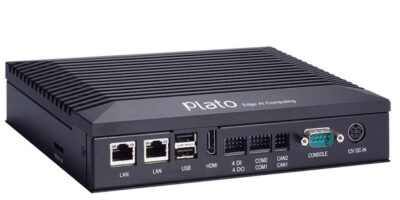
Axiomtek’s RSC100, ARM-based Edge embedded PC featuring the Hailo-8 AI accelerator is now available from industrial computing systems specialist, Impulse Embedded. The streamlined processing unit for AI applications can offer up to 26 T operations per second and is housed in a cost-effective, power-efficient unit, said the company. 

The edge system combined with Hailo’s Hailo-8 processor, can be used in a range of applications, including public safety, smart factory, agriculture and intelligent transportation.

The system chassis is made up of aluminium and heavy duty steel with an IP40 rating and supports a wide operating temperature of -20 to +70 degrees C, making it suitable for use in harsh, industrial environments where the temperatures can vary throughout operation. The RSC100 has dual Gigabit Ethernet ports, an M.2 3052 B-key slot which can be used to install a 5G module and two full-size miniPCIe slots. The RSC100 also has seven SMA antenna breakout holes for wireless comms requirements of a variety of applications.  

The eight-core ARM processor is backed up with 4Gbyte of LPDDR4 system memory and has 16Gbyte of eMMC storage onboard as standard as well as an M.2 2280 M-key SSD slot with PCIe x4 NVMe support and a MicroSD card slot for additional storage.  

Further I/O includes a built-in HDMI 2.0 port with 4K resolution support, two serial ports supporting RS-232/422/485, two CANbus ports, two USB2.0 ports and eight channels of digital I/O, (four, direct input, four direct output). For embedded operating system support, Yocto Linux 3.0 is supplied. 

The I/O, software and connectivity, combined with an AI-focused microprocessor that uses just 2.5W whilst achieving 26TOPs of INT-8 performance, means the RSC100 can process complex deep learning neural networks at the edge in smart embedded applications, explained Impulse Embedded. 

As with all of its embedded computing range, Impulse can configure the RSC100 to customer’s exact specifications in its UK-based engineering facility. It offers a choice of storage, peripheral cards, operating system, and neural network.   

The company has embedded systems capabilities and a team of in-house engineers and specialists to create revision-controlled systems which can reduce project costs and development time.  

http://www.impulse-embedded.co.uk 

> Read More

TSN Ethernet switches are turnkey for industrial automation

Believed to be the industry’s first turnkey devices for industrial automation networks, the Microchip’s LAN9668x family of time sensitive networking (TSN) switching devices delivers IEEE standards-compliant features to lower latency data traffic flows and greater clock accuracy.

Connected warehouses and other industrial ecosystems with converged IT and operational technology architectures rely on TSN and Ethernet for precise timing, synchronisation and connectivity of devices including cameras, barcode readers, scanners and conveyors. These ecosystems require next-generation network technology to interconnect device, sensor and equipment communication. The LAN9668 TSN switching devices deliver IEEE standards-compliant features and are complemented by Microchip’s LAN8814 quad-port Gigabit Ethernet (GbE) physical layer (PHY) transceiver. 

Microchip’s LAN9668-I / 9MX and LAN9668-9MX devices are eight-port switches for industrial and commercial applications, respectively, outfitted with Arm Cortex-A7 central processing units (CPUs), supporting TSN IEEE standards for communication in industrial settings. These include IEEE 1588v2 and IEEE 802.1AS-2020 for precision timing, IEEE 802.1Qci for per-stream filtering and policing, IEEE 802.1Qav and IEEE 802.1Qbv for traffic shaping and IEEE 802.1CB for seamless redundancy, as well as IEC-62439-2 (Media Redundancy Protocol) and ODVA-DLR and IEC-61158-6-10 for media redundancy. 

Microchip’s Ethernet Switch API (MESA) and PHY API (MEPA) enable designers to develop a comprehensive, user-friendly function library that is operating-system independent. The LAN9668 and LAN8814 scalable TSN chipsets are supported by Microchip’s software framework and provide the lowest latency and end-to-end transmission of communication traffic.

The LAN8814 is a quad-port GbE PHY that supports the latest TSN requirements including IEEE 1588 v2 and frame pre-emption. Designers using LAN9668 and LAN8814 technology can employ the TSN chipset to achieve timing, stream reservation, protection and management, to reduce both development time and cost.

“While devices and equipment previously required their own communication systems, TSN improves interoperability through connecting data streams to simplify traffic,” said Charles Forni, vice president of Microchip’s USB and networking business unit. “Enabling converged network architectures, this technology allows developers to expand their products into new markets and provide better performance in existing networks,” he added. 

Microchip also provides associated IStaX/SMBStaX and WebStaX network operating systems. They include a reproduceable reference design available as a board design or kit of Microchip parts including TSN switches, Ethernet PHYs, clock devices and oscillators. 

The LAN9668-I / 9MX and LAN9668-9MX TSN Ethernet switches are supported by the VSC6817SDK IStaX Linux application software, an industrial Ethernet switch software solution supporting Microchip’s managed Ethernet switch devices. The VSC6817SDK IStaX Linux network OS is an industrial Ethernet switch software which supports Microchip’s managed Ethernet switch devices. The SMBStaX Linux network OS and WebSTaX Linux network OS are available to commercial designers. These development tools are highly integrated with advanced L2+ switch features. 

Reference designs and evaluation boards also are available from Microchip and the company’s distribution partners.

The LAN9668/9MX and the LAN8814/ZMX are available in volume production.

http://www.microchip.com 

> Read More

Arm-based SoC and demo board are available to test Morello 

To test the Morello architecture, developed by Arm and the University of Cambridge, Arm has designed and developed an SoC and demonstrator board which contains the first example of the prototype architecture.  

The Morello programme has been a research initiative by a consortium led by Arm to design a new, inherently more secure, Arm-based computing platform. Arm has been collaborating with the University of Cambridge for several years on its CHERI Capability Hardware Enhanced RISC Instructions) architecture, which defines hardware capabilities that would provide a fundamentally more secure building block for software. 

The CHERI architectural extensions are designed to mitigate memory safety vulnerabilities, or software defects that are exploited by hackers to take control of a device or system – at a hardware level. CHERI augments pointers (the variables in computer code that reference where data is stored in memory) with limits as to how those references can be used, the address ranges that they can use to access and which functionality they can use to access.

These hardware capabilities are unique to the processor architecture. Once baked into silicon, they cannot be forged in software. Use of these capabilities in place of some or all the memory addresses can improve the spatial memory safety of software, particularly software written in C or C++ code.

These capabilities can also be used as a building block to allow the enforcement of much stronger temporal memory safety with potentially far lower overheads than current approaches to partitioning. Known as compartmentalisation, this process isolates different parts of critical code into individual ‘walled’ areas. Code operating within one compartment has no access to any other area; even if an attacker breaches one piece of the code or data, they are trapped within that one small zone.

These hardware capabilities will be fundamental in designing future devices that are resilient to memory corruption vulnerabilities and other forms of software-based exploitation, explained Arm.

The Morello prototype boards are ready for software developers and security specialists to start exploring the security advances possible with the Morello architecture.

The limited-edition boards are based on the Morello prototype architecture embedded into an Armv8.2-A processor (an adaptation of the Arm Neoverse N1 processor). The boards are being distributed to major stakeholders, such as Google and Microsoft, as well as to interested partners in industry and academia via the UKRI Digital Security by Design (DSbD) initiative to test the hypothesis of Morello and discover if this is a viable security architecture for businesses and consumers.

The Arm Morello research program aims to create a more secure hardware architecture for processors. Its architectural extensions are based on the CHERI protection model.

The Morello program aims to assess the viability of the prototype hardware SoC employing unique extensions to the conventional Arm hardware instruction set that improve device security. 

“Computers are incredibly useful but the price we pay for that utility is more and more exposure to security and privacy issues,” said Ben Laurie, principal engineer, Security, Google Research. “CHERI can allow for better, more cost-effective protection without reduced performance and Arm’s Morello prototype can help mitigate security issues showing the way to a better future for all computer users,” he said.

David Weston, director of Enterprise and OS Security at Microsoft, declared he is excited about the Morello project. “Memory safety exploits are one of the longest standing and most challenging problems in all of software security,” he said. “Using core silicon architecture to eliminate whole classes of security issues with minimal performance impact has the opportunity to be transformative with massive positive impact”.

The next two years will see the ecosystem testing, writing code and collaboratively providing critical feedback to determine whether any features will be used in future versions of the Arm architecture, said Arm. If the Morello prototype architecture performs as expected, it will be fundamental in future processor designs, protecting businesses, individuals and the devices of tomorrow.

http://www.arm.com

> Read More

Industrial edge inference server is ready for rapid deployment

Powered by Nvidia’s A2 Tensor core GPU, the HPC-6240+ASMB-622 industrial edge inference server has been designed for rapid deployment, management, and scaling of AI and inference workloads in the hybrid cloud, says Advantech.

The HPC-6240+ASMB-622, powered by the soon to be available Nvidia A2, has a depth of 20.5 inch (520mm) depth and multiple expansion slots. 

Enterprises can confidently deploy hardware that securely and optimally runs accelerated workloads while using the Nvidia AI platform for inference, explained Advantech. Nvidia AI for inference includes software such as Nvidia Triton Inference Server and Nvidia TensorRT.

The server is therefore suitable for industrial equipment manufacturers (IEM), robotics, retail, intelligent video analytics (IVA), and other applications of AI at the edge.

The Nvidia A2 GPU’s compact size and low power requirements exceed the demands for edge deployments at scale, said Advantech. Combined with the HPC-6240+ASMB-622, it can deliver up to 20x higher inference performance versus CPUs and 1.3x more efficient IVA deployments than previous GPU generations, at an entry-level price point, added Advantech. 

The HPC-6240+ASMB-622 is a 2U, short-depth compact edge server with dual third Gen Intel Xeon scalable processors. It provides eight expansion slots and multiple PCIe for flexible GPU, network interface controller (NIC), frame grabber card and motion control card integrations. Four PCIe x16 design supports up to four Nvidia A2 GPUs for AI and high performance computing (HPC). 

The low power budget, compact size and multiple expansion capability with four A2 GPUs enables the server to be used for complex AI auto-optical inspection and manufacturing equipment applications.

The thermal management system increases airflow and pressure to enable high computing workloads at the industrial edge by cooling GPU cards and reducing noise output. 

The HPC-6240+ASMB-622 server is able to scale out from a single-GPU node to multi-GPU nodes when needed in industrial applications, especially for AOI, voice recognition and translation.

The HPC-6240+ASMB-622 is available now.  

Advantech specialises in IoT intelligent systems and embedded platforms. To embrace the trends of IoT, big data, and artificial intelligence, it promotes IoT hardware and software solutions with the Edge Intelligence WISE-PaaS core to assist business partners and clients in connecting industrial chains. 

http://www.advantech.eu 

> Read More

About Smart Cities

This news story is brought to you by smartcitieselectronics.com, the specialist site dedicated to delivering information about what’s new in the Smart City Electronics industry, with daily news updates, new products and industry news. To stay up-to-date, register to receive our weekly newsletters and keep yourself informed on the latest technology news and new products from around the globe. Simply click this link to register here: Smart Cities Registration