Ryzen Embedded R2000 has 2x cores for IoT, says AMD

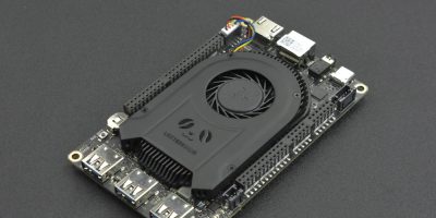
Equipped with up to two times as many cores as the previous generation of Ryzen Embedded SoC processors, the Ryzen Embedded R2000 series targets industrial and robotics systems, machine vision, the IoT and thin client equipment, said AMD.

The R2514, for example has up to 81 per cent higher CPU and graphics performance than the comparable R1000 series processor, confirmed AMD. Performance-per-watt efficiency is also optimised using Zen+ core architecture with AMD Radeon graphics for multimedia capabilities. Ryzen Embedded R2000 processors can power up to four independent displays in 4K resolution.

Embedded R2000 Series processors are scalable up to four Zen+ CPU cores with eight threads, 2Mbyte of L2 cache and 4Mbyte of shared L3 cache, allowing embedded system designers can scale performance and power efficiencies with a single processing platform, said the company. The Ryzen Embedded R2000 also supports up to 3200Mtransfer per second DDR4 dual channel memory and expanded I/O connectivity, to deliver 33 per cent higher memory bandwidth and up to two times greater I/O connectivity compared to R1000 series processors. 

The series is suitable for industrial applications like robotics and machine vision as well as thin clients and mini-PCs, which require performance, optimised power and graphics, commented the company. 

They can power up to four independent displays in 4K resolution leveraging DisplayPort 1.4, HDMI 2.0b or eDP 1.3 interfaces. They also feature peripherals and interfaces with up to 16 lanes of PCIe Gen3, two SATA 3.0 and six USB ports (USB 3.2 Gen2 and 2.0).

OS support includes Microsoft Windows 11/10, and Linux Ubuntu LTS.

 The series consists of the R2324 and R2312 SoC processors which are in production now and the R2544 andR2541 which are expected to be available in October 2022. Planned product availability extends up to 10 years, providing customers with a long-lifecycle support roadmap

http://www.amd.com 

> Read More

Tensilica DSP IP cores target radar and lidar

Two IP cores have been added to the Tensilica ConnX family of DSPs by Cadence. Intended for embedded processing in automotive, consumer and industrial markets, the ConnX 110 and ConnX 120 DSPs’ architecture is optimised for small memory footprint and low-power signal processing. The ConnX 110 and ConnX 120 DSPs share a common instruction set architecture (ISA) with the ConnX B10 and B20 DSPs preserving software compatibility for easy migration. 

The 128-bit ConnX 110 DSP and 256-bit ConnX 120 DSP feature an N-way programming model an, like the rest of the Tensilica DSP portfolio, support the Tensilica Instruction Extension (TIE) language, which allows customers to tailor the instruction set, add specialised data types, and implement tightly integrated interfaces between the DSP and external logic. 

The new DSPs are supported by a comprehensive set of complex math library functions in the NatureDSP, Eigen and Radar libraries. As with all existing ConnX DSPs, they are automotive-ready with full ISO 26262 compliance to ASIL-D with FlexLock or to ASIL-B.

The Tensilica ConnX 110 and 120 DSPs have an optimised instruction set for radar, lidar and communications applications. They also feature optional acceleration operations for linear-feedback shift, convolutional encoding, single peak search and dual peak search. The 128-bit (ConnX 110) and 256-bit (ConnX 120) SIMD are suitable for complex math operations based on eight-, 16- and 32-bit fixed-point and half-, standard- and double-precision floating-point.

The ConnX 120 additionally offers Viterbi and Turbo decoders.
NXP uses Cadence Tensilica DSP cores for its ADAS (advanced driver assistance system) product offerings, said Robert Dunnigan, director program management ADAS at NXP Semiconductors. 

Another customer, indie Semiconductor develops multiple sensor modalities “in the pursuit of the uncrashable car”. Lionel Federspiel, executive vice president of engineering for indie Semiconductor, commented: “Cadence’s Tensilica ConnX processor family in conjunction with indie’s architecture is ideally suited to implement unique design solutions with high performance, low power, and gate count optimisation. As a pure-play automotive solutions innovator, quality and reliability are essential to the success of our products.”

“Radar and communications processing trends require solutions that perform more processing in less time,” explained David Glasco, vice president of research and development for Tensilica IP at Cadence. “Automotive radar demands multi-antenna, high-resolution systems with rapid response. Similarly, 5G wireless communications requires much higher data rates and lower latencies than previous generations. The Tensilica ConnX 110 and ConnX 120 DSPs meet these demands by extending the already-efficient processing capability of the ConnX DSPs and enhancing them with even more fixed- and floating-point complex data processing capacity at low power and area.”

http://www.cadence.com

> Read More

ANS-8A64 server protects data centres to IPSec

The ANS-8A64 server series is based on an Intel Atom C3000 processor, which qualifies it for network acceleration system for software defined wide area network (SD-WAN) users, said Portwell. 

SD-WAN is used to connect a wide range of corporate networks, data centres, internet applications and cloud services, which aims to help reduce a WAN’s operating cost and improve connection flexibility, explained Portwell. More and more applications will depend on the cloud to process data, which also brings the escalating demands for network security as this data on the cloud may contain personal ID, credit card numbers and other private information. 

IPSec protocol works in the third layer of the OSI (open systems interconnection) model and supports two modes, host-to-host mode and tunnel mode, either of which can be used to build a virtual private network (VPN) to increase the security of network transmission.

The Intel Atom C3000 processor series features industry-leading performance per watt, claimed Portwell, with low thermal design power (TDP) and configurable high-speed I/O, making it suitable for networks, storage devices, IoT and scalable designs. It is also equipped with Intel QuickAssist Technology (Intel QAT). The Intel QAT engine means IPSec protocol operation, data encryption, decryption and compression can be handled independently. It saves the CPU resource for other critical workloads and eventually optimises the overall work efficiency and performance, said Portwell.  

During field tests of the data plane development kit (DPDK) and Intel QAT, the ANS-8A64 was used as IPSec gateways and the encryption and decryption performance was repeatedly tested. 

In a one-way test, packets are sent unidirectionally from server port1 to server port2, and encryption and decryption are performed by IPSec gateway1 and IPSec gateway2.

A two-way test, consists of the server port1 and server port2 sending packets at the same time, and encrypting and decrypting packets through IPSec gateway1 and IPSec gateway2.

Portwell reported that the hardware acceleration engine, Intel QAT offers a “significant system optimisation and effectively betters the overall performance in both one-way and two-way testing”. 

Portwell is an Associate member of the Intel Internet of Things Solutions Alliance, designs and manufactures a full range of IPC products (SBC, backplane, redundant power supply, rack mount and node chassis), embedded architecture solutions, DVR system platforms and communications appliances. It provides R&D and project management services to decrease customers’ time to market and reduce project risk and cost. Portwell is also an ISO 13485, ISO 9001 and ISO 14001 -certified company that deploys quality assurance through product design, verification and manufacturing cycles. 

http://www.portwell.eu 

> Read More

Eight-bit MCU development board connects to 5G LTE-M NB-IoT networks

Microchip Technology’s AVR-IoT cellular mini development board is the latest to join its ABR family. It is based on the AVR128DB48 eight-bit microcontroller (MCU). It provides a platform to start building sensor and actuator nodes on 5G narrowband IoT (NB-IoT) networks.  

The small form factor board aimed at developers who want to connect IoT devices to an available 5G network. This is an essential feature for devices on the go or located in remote areas with limited availability of long range (LoRa) networks or other low power wide area networks (LPWAN). 

The AVR128DB48 eight-bit MCU family includes security protection with Microchip’s ATECC608 CryptoAuthentication device. The ATECC608 can be configured to most major cloud service providers through Microchip’s IoT provisioning tool. 

“Microchip continues to expand its family of AVR eight-bit MCUs for developers to implement a variety of embedded designs with ease and flexibility,” said Greg Robinson, vice president of marketing for Microchip’s eight-bit MCU business unit. 

The ability to connect remote and mobile devices to a 5G narrowband network with an eight-bit MCU opens up new opportunities for battery-operated devices due to the low power combined with high-quality analogue peripherals, he added.

The AVR-IoT cellular mini development board comes pre-configured to send data from on-board light and temperature sensors to the cloud, viewable using Microchip’s sandbox portal. The sandbox portal lets customers track and monitor their device in real time from a remote location. 

This functionality covers the core requirements of many applications in various industries including agriculture, industrial and energy, as well as consumer spaces such as transportation of goods, alarm systems, building automation and remote monitoring. 

To provide an easier, more efficient and more cost-effective solution for connecting IoT devices to 5G using the AVR128DB48 MCU, Microchip has partnered with Sequans to include its Monarch 2 GM02S single-chip radio equipped with 5G LTE-M and narrowband IoT. Microchip also partnered with Truphone to provide the SIM card for cellular service that offers coverage worldwide. 

The Monarch 2 GM02S is a 5G-ready LTE-M and NB-IoT solution on a single chip, designed specifically for NB-IoT applications, including sensors, wearables and other low data, low power devices. By partnering with Microchip on its AVR-IoT cellular board, Sequans claimed to simplify and lower the costs of IoT device design.

“Owning and operating all elements of the eSIM ecosystem in-house coupled with access to a large number of low-power cellular networks through a single SIM SKU, provides Microchip customers looking to connect IoT devices a future proof cellular service.” said Steve Alder, chief business development officer of Truphone.

The AVR-IoT cellular mini development board fits the Adafruit Feather form factor. It features a Qwiic/Stemma I2C connector for easy functionality extension, creating a clear path to production. It is also Arduino-compatible and is supported by Microchip’s Github Library, which provides functionality for HTTPS, MQ telemetry transport (MQTT), and low power.   

Users can access the Microchip sandbox page for a tutorial on how to get up and running and establish a connection with the AVR-IoT cellular mini development board.

Microchip Technology provides smart, connected and secure embedded control, serving more than 120,000 customers across the industrial, automotive, consumer, aerospace and defence, communications and computing markets. Headquartered in Chandler, Arizona, Microchip offers technical support along with dependable delivery and quality. 

https://www.microchip.com

> Read More

About Smart Cities

This news story is brought to you by smartcitieselectronics.com, the specialist site dedicated to delivering information about what’s new in the Smart City Electronics industry, with daily news updates, new products and industry news. To stay up-to-date, register to receive our weekly newsletters and keep yourself informed on the latest technology news and new products from around the globe. Simply click this link to register here: Smart Cities Registration