Renesas launches RZ/G3S 64-bit microprocessor with enhanced peripherals for IoT Edge and gateway devices

As the latest addition to Renesas’ RZ/G Series MPU, the RZ/G3S is designed to meet the demanding requirements of modern IoT devices, offering power consumption as low as 10µW (microwatts) in standby mode and fast startup for the Linux operating system. The new MPU comes with a PCI Express interface that enables high-speed connectivity with 5G wireless modules. Additionally, the device boasts enhanced security features such as tamper detection to ensure data security. These features make the device ideal for IoT applications such as home gateways, smart meters, and tracking devices.

“Renesas’ RZ/G has seen a steady increase in adoption in the global industrial human machine interface market,” said Daryl Khoo, Vice President of Embedded Processing 1st Division at Renesas. “The RZ/G3S represents the next generation products that will extend our reach to the rapidly growing 5G IoT and Gigabit Wi-Fi 7 gateway markets. Renesas has been aggressively expanding our connectivity portfolio in these markets through strategic acquisitions to offer advanced connectivity solutions that are power efficient at the system level and enhance data utilisation.”

The RZ/G3S employs an Arm Cortex-A55 core as the main CPU with a maximum operating frequency of 1.1 GHz and two Cortex-M33 cores as sub-CPUs operating at 250 MHz. Users can distribute the MPU’s workloads to sub-CPUs, allowing the device to efficiently handle tasks such as receiving data from sensors, controlling system functions and managing power systems. This reduces the workload on the main CPU, resulting in fewer components, lower costs and a smaller system size.

The device’s newly added power management system is designed to reduce power consumption to extremely low levels — less than 10 µW. The MPU also supports the DDR self-refresh function which allows to retain DRAM data, while also enabling fast Linux startup. The fast startup allows IoT devices, which frequently operate intermittently, to save power and significantly extend the runtime of battery-powered devices. Moreover, the device offers a standby mode that can maintain sub-CPU operation at a power level as low as 40 mW, offering the flexibility to optimise power consumption based on the specific operating requirements of each application.

The RZ/G3S is equipped with a wide range of peripheral functions including Gigabit Ethernet, CAN, USB, as well as the PCI Express interface. By connecting with 5G communication modules, the device can achieve high-speed communication at Gigahertz levels.

Similar to other RZ/G devices, the RZ/G3S features an ECC (Error Correction Code) function in both internal memory and external DDR interface to maintain data integrity. The Verified Linux Package (VLP) based on the industrial-grade Linux software (Civil Infrastructure Platform™ (CIP) Linux) is available for the RZ/G3S. With VLP, developers receive over 10 years of maintenance support, ensuring long-term protection against security threats. The device also provides tamper detection along with secure boot, secure debug and more. RZ/G series products are already Level 2 PSA Certified from Arm and Renesas has plans to include the RZ/G3S in the future.

Renesas has combined the new RZ/G3S MPU with optimised power management ICs and clock products to develop the “Single Board Computer Gateway”. The RZ/G3S’s rich set of interfaces allows the device to connect with various sensors via USB, CAN, RS485, UART, and I2C. It also offers high performance wireless connectivity options to build a robust network for home automation or IoT applications. Its multicore design allows for real-time processing of data while being power efficient with its advanced sleep mode functions. The Winning Combinations are technically vetted system architectures from mutually compatible devices that work together seamlessly to bring an optimised, low-risk design for faster time to market. Renesas offers more than 400 Winning Combinations with a wide range of products from the Renesas portfolio to enable customers to speed up the design process and bring their products to market more quickly. They can be found at renesas.com/win.

https://www.renesas.com/rzg3s

> Read More

GaN FETs Enable 75 – 231 ampere laser diode control in nanoseconds for advanced automotive autonomy

EPC introduces three evaluation boards – EPC9179, EPC9181, and EPC9180 – featuring pulse current laser drivers of  75 A, 125 A, and 231 A , showcasing EPC’s AEC-Q101 GaN FETs. These FETs; EPC2252, EPC2204A, and EPC2218A are 30% smaller and more cost-effective than their predecessors. Designed for both long and short-range automotive lidar systems, these boards expedite solution evaluation with varied input and output options.

All boards share identical functionality, differing only in peak current and pulse width. Utilising a resonant discharge power stage, they employ a ground-referenced GaN FET driven by LMG1020 gate driver. The GaN FET’s ultrafast switching enables rapid discharge of a charged capacitor through the load’s stray inductance, enabling peak discharge currents of tens to hundreds of amps within nanoseconds. The printed circuit board is designed to minimise power loops and common source inductance while offering mounting flexibility for laser diodes or alternative loads. To enhance user-friendliness, all boards ship with EPC9989 interposer PCBs, featuring various footprints to accommodate a variety of laser diodes or other loads. Customers can choose one that meets their needs to evaluate the GaN solutions.

The EPC9179/81/80 boards are designed to be triggered from 3.3V logic or differential logic signals such as LVDS. For single-ended inputs, the boards can operate with input voltages down to 2.5 V or 1.8 V with a simple modification. Designing an automotive lidar system is complex, and finding a reliable solution is challenging. The purpose of these evaluation boards is to simplify the evaluation of powerful GaN-based lidar drivers that switch faster and deliver higher pulse current than other semiconductor solutions. For technical details, EPC offers full schematics, bill of materials (BOM), PCB layout files, and a quick start guide on EPC’s website.

“To meet the growing demand for automotive lidar, these cost-effective boards, featuring our latest AEC products, streamline evaluation, reducing time-to-market with exceptional switching performance,” said Alex Lidow, CEO, and co-founder of EPC.

https://epc-co.com

> Read More

u-blox module unlocks new automotive use cases

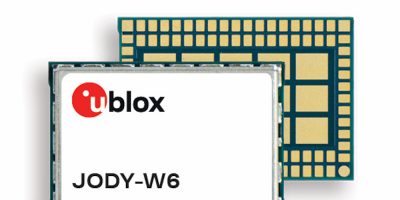
u-blox has announced JODY-W6, a concurrent dual-band Wi-Fi 6E module with Bluetooth 5.3, including LE Audio, in a compact size (13.8 x 19.8 x 2.5 mm). The new module targets automotive use cases in infotainment and navigation, advanced telematics, as well as OEM telematics.

According to the TSR (Techno Systems Research CO. LTD.) Wireless Connectivity Market Report, Wi-Fi 6 and 6E technologies are experiencing significant and promising growth in the automotive industry. Wi-Fi 6 focuses on efficiency, with reduced data congestion, improved network capacity, and lower overall power consumption. Instead, Wi-Fi 6E focuses on spectrum, enabling more concurrent users, reduced congestion, and enhanced security.

Not only does the u-blox JODY-W6 deliver the benefits of Wi-Fi 6E, but it also features dual-mode Bluetooth with LE Audio. JODY-W6 is globally certified and can withstand operating temperatures from -40 °C up to 105 °C.

The module is available with either two or three antennas. Upon request, it can also integrate an LTE filter. An EVK and an M.2 card will be available for the JODY-W6 series. Furthermore, its compatibility with previous JODY modules to ensure seamless scalability.

“JODY-W6 is a smart and reliable solution that helps overcome congestion and fulfils scalability requirements through its highly adaptable compact size. Specific use cases include support for AppleCarPlay and AndroidAuto, personalised entertainment, data off-loading, and smart/roof-integrated antennas.

The u-blox JODY-W6 comes equipped with an embedded NXP Semiconductors AW693 chipset.

“The AW693 SoC (System-on-Chip) embedded in the automotive JODY-W6 SoM (System-on-Module) leverages the latest concurrent dual-band Wi-Fi 6E and Bluetooth LE audio technologies to unlock new opportunities for a wide variety of use cases and businesses in the automotive domain. The AW693 chipset is packed with advanced features, including MU-MIMO, OFDMA, and target wake time (TWT), allowing the u-blox JODY-W6 compact module to benefit from the synergy of our gold partnership,” says Larry Olivas, Vice President and General Manager of Wireless Connectivity Solutions, NXP Semiconductors.

https://www.u-blox.com

> Read More

NXP and MicroEJ collaborate to use software containers to accelerate embedded platform development

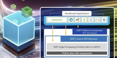
NXP Semiconductors has announced the NXP Platform Accelerator, developed in collaboration with MicroEJ. The NXP Platform Accelerator leverages MICROEJ VEE software containers with standard APIs to bring a smartphone-like software design process experience to the industrial and IoT edge. The use of MICROEJ VEE enables software portability across NXP’s broad portfolio of RTOS-based MCUs and Linux-based applications processors, enabling manufacturers to significantly accelerate new product development and reduce costs. Furthermore, the NXP Platform Accelerator provides dedicated APIs to create easy access to advanced functionalities integrated in NXP’s processor portfolio, such as power management and 3D/2D graphics.

Why it matters: Smart devices across industrial and IoT markets are challenging to develop and deploy. Many are designed for a single purpose, with fixed functionality and limited computing capability that may be insufficient to support the evolving needs of an increasingly automated environment. Scaling product capability requires redeveloping and integrating low-level software, RTOS or higher-level OS, and middleware, which can create major development challenges and significantly slow product development.

The NXP Platform Accelerator solves this challenge by utilising software containerisation that enables binary software portability across the breadth of NXP’s processors portfolio, from MCUs to applications processors. Reusability at the binary level enables customers to prototype new products as quickly as possible and create a broad portfolio of complex smart devices that evolve with market needs and trends. Furthermore, the NXP Platform Accelerator enables sandboxed application deployment at the edge, bringing smartphone-like capability to the edge, such as partial or complete over-the-air updates, downloadable apps, and microservices.

More details: “Just like what happened in the smartphone industry, containerisation can be a tremendous tool to drive the rapid development of new smart device platforms,” said Charles Dachs, Senior Vice President and General Manager, Industrial and IoT Edge, NXP. “By integrating MicroEJ’s software container with NXP’s broad portfolio of edge processing solutions, we equip engineers to bring more products to market faster, with reduced costs, and to support the continuous evolution of their smart devices across industrial and IoT markets.”

“Software portability and BoM optimisation are often mutually exclusive,” said Fred Rivard, CEO of MicroEJ. “The NXP Platform Accelerator combines these two objectives, thanks to tiny software containers. This small-footprint innovation allows developers to benefit from both an optimised bill of materials and a modern software design process. This enables engineers to create new products and platforms more quickly, design products that are lower power and lower cost, while still allowing for feature-rich differentiation and innovation by device manufacturers.”

The NXP Platform Accelerator integrates advanced development tools, including simulation, virtual device management and a multi-language framework for combination of C, Java, and JavaScript languages, as well as agile collaboration processes and support for Android Studio, IntelliJ and Eclipse IDEs. In addition, the NXP Platform Accelerator integrates dedicated APIs for power management and graphic functions, making it extremely easy for customers to utilise the complex and powerful hardware IP brought by NXP. For example, a simple call to “low power profile” from the customer application layer will trigger performance optimisation for a given power profile. In addition, NXP-tailored containers support broad scalability and integrate NXP-specific optimisations and libraries that leverage processor hardware innovations.

The NXP Platform Accelerator is currently available for NXP’s processors, including power-efficient i.MX RT595 and high-performance multi-core i.MX RT1170 crossover MCUs.

http://nxp.com/PlatformAccelerator

> Read More

About Smart Cities

This news story is brought to you by smartcitieselectronics.com, the specialist site dedicated to delivering information about what’s new in the Smart City Electronics industry, with daily news updates, new products and industry news. To stay up-to-date, register to receive our weekly newsletters and keep yourself informed on the latest technology news and new products from around the globe. Simply click this link to register here: Smart Cities Registration