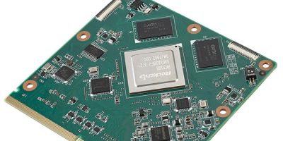
IMDT launches new SOM and SBC with the latest Renesas RZ/V2H SOC

IMDT has announced a new line of power-efficient, cost-effective and ready-to-use system-on-module (SOM) and single-board-computer (SBC) solutions, based on the new Renesas RZ/V2H microprocessor.

The IMDT Renesas V2H-based family of products delivers advanced functionality and high performance for Robotic, IoT and industrial applications. Equipped with a powerful, Arm-based CPU and Renesas proprietary AI accelerator, these products support diverse uses, including high-bandwidth communications, machine learning, and high-definition image processing.

The RZ/V2H processor features Renesas’s proprietary AI accelerator, the DRP (Dynamically Reconfigurable Processor)-AI3, which boasts a power efficiency of 10 TOPS/W. Additionally, it integrates four Arm Cortex-A55 CPU cores that reach a maximum operating frequency of 1.8 GHz, tailored for Linux application processing. For high-performance real-time processing, it includes two Cortex-R8 cores operating at 800 MHz, alongside one Cortex-M33 core serving as a subcore. By integrating these cores into a single chip, the device effectively manages both vision-AI and real-time control tasks, making it ideal for demanding robotics applications.

The IMDT V2H based SOM supports 4 x 4-lane MIPI CSI-2 connections, enabling attachment of up to four cameras. Additionally, the full module provides customisable options such as onboard Wi-Fi/Bluetooth, various memory and storage capacities, and PHY configurations, allowing users to tailor the system to their specific needs. The IMDT V2H SBC carrier board transforms the IMDT V2H SOM into a compact, high-performance mini-computer. Measuring only 125 x 80 x 20 mm, this fully customisable small form factor SBC features a cost-effective system design, ideal for diverse applications in robotics, drones, and smart city projects. The V2H SBC provides a multitude of assembly options, personalised and adjusted to meet specific customer needs, alongside comprehensive onboard connectivity. It presents developers with an energy-efficient solution that occupies minimal space.

https://www.imd-tec.com

Written by Annie Shinn

> Read More

Renesas unveils powerful single-chip MPU for next-gen robotics

Renesas Electronics Corporation, has expanded its popular RZ Family of microprocessors (MPUs) with a new device targeting high-performance robotics applications, the RZ/V2H enables both vision AI and real-time control capabilities.

The device comes with a new generation of Renesas proprietary AI accelerator, DRP (Dynamically Reconfigurable Processor)-AI3, delivering 10 TOPS/W power efficiency, a 10-fold improvement over previous models. Additionally, pruning technology employed in the DRP-AI3 accelerator significantly improves AI computing efficiency, boosting AI inference performance up to 80 TOPS. This performance boost allows engineers to process vision AI applications directly at edge AI devices without relying on cloud computing platforms.

The RZ/V2H incorporates four Arm Cortex-A55 CPU cores with a maximum operating frequency of 1.8 GHz for Linux application processing, two Cortex-R8 cores running at 800 MHz for high-performance real-time processing, and one Cortex-M33 as a sub core. By integrating these cores into a single chip, the device can effectively manage both vision AI and real-time control tasks, making it ideal for demanding robotics applications of the future. Since the RZ/V2H consumes less power, it eliminates the need for cooling fans and other heat-dissipating components. This means engineers can design systems that are smaller in size, less expensive, and more reliable.

Renesas has applied its proprietary DRP technology to develop the OpenCV Accelerator that speeds up the processing of OpenCV, an open-source industry standard library for computer vision processing. The resulting speed improvement is up to 16 times faster compared to CPU processing. The combination of the DRP-AI3 and the OpenCV Accelerator enhances both AI computing and image processing algorithms, enabling the power-efficient, real-time execution of Visual SLAM used in applications such as robot vacuum cleaners.

To accelerate development, Renesas also released AI Applications, a library of pre-trained models for various use cases, and the AI SDK (Software Development Kit) for rapid development of AI applications. By running these software on the RZ/V2H’s evaluation board, engineers can evaluate AI applications easily and earlier in the design process, even if they do not have extensive knowledge of AI.

https://www.renesas.com/rzv2h

> Read More

Renesas develops new AI accelerator for lightweight AI models

Renesas has announced the development of embedded processor technology that enables higher speeds and lower power consumption in microprocessor units (MPUs) that realise advanced vision AI.

The newly developed technologies are a dynamically reconfigurable processor (DRP)-based AI accelerator that efficiently processes lightweight AI models, and Heterogeneous architecture technology that enables real-time processing by cooperatively operating processor IPs, such as the CPU.

Renesas produced a prototype of an embedded AI-MPU with these technologies and confirmed its high-speed and low-power-consumption operation. It achieved up to 16 times faster processing (130 TOPS) than before the introduction of these new technologies, and world-class power efficiency (up to 23.9 TOPS/W at 0.8 V supply).

Amid the recent spread of robots into factories, logistics, medical services, and stores, there is a growing need for systems that can autonomously run in real time by detecting surroundings using advanced vision AI. Since there are severe restrictions on heat generation, particularly for embedded devices, both higher performance and lower power consumption are required in AI chips. Renesas developed new technologies to meet these requirements.

As a typical technology for improving AI processing efficiency, pruning is available to omit calculations that do not significantly affect recognition accuracy. However, it is common that calculations that do not affect recognition accuracy randomly exist in AI models. This causes a difference between the parallelism of hardware processing and the randomness of pruning, which makes processing inefficient.

To solve this issue, Renesas optimised its unique DRP-based AI accelerator (DRP-AI) for pruning. By analysing how pruning pattern characteristics and a pruning method are related to recognition accuracy in typical image recognition AI models (CNN models), we identified the hardware structure of an AI accelerator that can achieve both high recognition accuracy and an efficient pruning rate, and applied it to the DRP-AI design. In addition, software was developed to reduce the weight of AI models optimised for this DRP-AI. This software converts the random pruning model configuration into highly efficient parallel computing, resulting in higher-speed AI processing. In particular, Renesas’ highly flexible pruning support technology (flexible N:M pruning technology), which can dynamically change the number of cycles in response to changes in the local pruning rate in AI models, allows for fine control of the pruning rate according to the power consumption, operating speed, and recognition accuracy required by users.

This technology reduces the number of AI model processing cycles to as little as one-sixteenth of pruning incompatible models and consumes less than one-eighth of the power.
Robot applications require advanced vision AI processing for recognition of the surrounding environment. Meanwhile, robot motion judgment and control require detailed condition programming in response to changes in the surrounding environment, so CPU-based software processing is more suitable than AI-based processing. The challenge has been that CPUs with current embedded processors are not fully capable of controlling robots in real time. That is why Renesas introduced a dynamically reconfigurable processor (DRP), which handles complex processing, in addition to the CPU and AI accelerator (DRP-AI). This led to the development of heterogeneous architecture technology that enables higher speeds and lower power consumption in AI-MPUs by distributing and parallelising processes appropriately.

A DRP runs an application while dynamically changing the circuit connection configuration between the arithmetic units inside the chip for each operation clock according to the processing details. Since only the necessary arithmetic circuits operate even for complex processing, lower power consumption and higher speeds are possible. For example, SLAM (Simultaneously Localisation and Mapping), one of the typical robot applications, is a complex configuration that requires multiple programming processes for robot position recognition in parallel with environment recognition by vision AI processing. Renesas demonstrated operating this SLAM through instantaneous program switching with the DRP and parallel operation of the AI accelerator and CPU, resulting in about 17 times faster operation speeds and about 12 times higher operating power efficiency than the embedded CPU alone.

Renesas created a prototype of a test chip with these technologies and confirmed that it achieved the world-class, highest power efficiency of 23.9 TOPS per watt at a normal power voltage of 0.8 V for the AI accelerator and operating power efficiency of 10 TOPS per watt for major AI models. It also proved that AI processing is possible without a fan or heat sink.
Utilising these results helps solve heat generation due to increased power consumption, which has been one of the challenges associated with the implementation of AI chips in a variety of embedded devices such as service robots and automated guided vehicles. Significantly reducing heat generation will contribute to the spread of automation into various industries, such as the robotics and smart technology markets. These technologies will be applied to Renesas’ RZ/V series—MPUs for vision AI applications.

https://renesas.com.

> Read More

Renesas announces ultra-fast MRAM test chip for IoT and AI devices

Renesas has announced that it has developed circuit technologies for an embedded spin-transfer torque magnetoresistive random-access memory (STT-MRAM, hereinafter MRAM) test chip with fast read and write operations. Fabricated using a 22-nm process, the microcontroller unit (MCU) test chip includes a 10.8-megabit (Mbit) embedded MRAM memory cell array. It achieves a random read access frequency of over 200 MHz and a write throughput of 10.4-megabytes-per-second (MB/s).

As IoT and AI technologies continue to advance, MCUs used in endpoint devices are expected to deliver higher performance than ever. The CPU clock frequencies of high performance MCUs are in the hundreds of MHz, so to achieve greater performance, read speeds of embedded non-volatile memory need to be increased to minimise the gap between them and CPU clock frequencies. MRAM has a smaller read margin than the flash memory used in conventional MCUs, making high speed read operation more difficult. On the other hand, for write performance, MRAM is faster than flash memory because it requires no erase operation before performing write operations. However, shortening write times is desirable not only for everyday use, but also for cost reduction of writing test patterns in test processes and writing control codes by end product manufacturers.

MRAM reading is generally performed by a differential amplifier (sense amplifier) to determine which of the memory cell current or the reference current is larger. However, because the difference in memory cell currents between the 0 and 1 states (the read window) is smaller for MRAM than for flash memory, the reference current must be precisely positioned in the centre of the read window for faster reading. The newly developed technology introduces two mechanisms. The first mechanism aligns the reference current in the centre of the window according to the actual current distribution of the memory cells for each chip measured during the test process. The other mechanism reduces the offset of the sense amplifier. With these adjustments, faster read speed is achieved.

Furthermore, in conventional configurations, there is large parasitic capacitance in the circuits used to control the voltage of the bitline so it does not rise too high during read operations. This slows the reading process, so a Cascode connection scheme is introduced in this circuit to reduce parasitic capacitance and speed up reading.

Thanks to these advances, Renesas can achieve the world’s fastest random read access time of 4.2 ns. Even taking into consideration the setup time of the interface circuit that receives the MRAM output data, we can realize the random read operation at frequencies in excess of 200 MHz.

For the write operation, the high-speed write technologies for embedded STT-MRAM announced in December 2021 improved write throughput by first applying write voltage simultaneously to all bits in a write unit using a relatively low write voltage generated from the external voltage (IO power) of the MCU chip through a step-down circuit, and then used a higher write voltage only for the remaining few bits that could not be written. This time, Renesas takes into account that because the power supply conditions used in test processes and by end product manufacturers are stable, the lower voltage limit of the external voltage can be relaxed. Thus, by setting the higher step-down voltage from the external voltage to be applied to all bits in the first phase, write throughput can be improved 1.8-fold.

Combining the above new technologies, a prototype MCU test chip with a 10.8Mbit MRAM memory cell array was fabricated using a 22 nm embedded MRAM process. Evaluation of the prototype chip confirmed that it achieved a random read access frequency of over 200 MHz and a write throughput of 10.4 MB/s at a maximum junction temperature of 125°C.

The test chip also contains 0.3 Mbit of OTP (Note 2) that uses MRAM memory cell breakdown to prevent falsification of data. This memory can be used to store security information. Writing to OTP requires a higher voltage than writing to MRAM, making it more difficult to perform writing in the field, where power supply voltages are often less stable. However, by suppressing parasitic resistance within the memory cell array, this new technology also makes writing in the field possible.

https://www.renesas.com

> Read More

About Smart Cities

This news story is brought to you by smartcitieselectronics.com, the specialist site dedicated to delivering information about what’s new in the Smart City Electronics industry, with daily news updates, new products and industry news. To stay up-to-date, register to receive our weekly newsletters and keep yourself informed on the latest technology news and new products from around the globe. Simply click this link to register here: Smart Cities Registration