Bridgetek adds Mood Lighting to PanL building automation platform

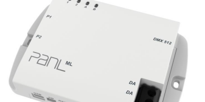
Convenient and cost-effective RGB-enabled lighting control can be implemented, says Bridgetek at the launch of its PanL Mood Lighting (ML) units.

The units extend the PanL home/building automation platform and comply with both DALI and DMX digital interface protocols. The ML units offer users complete control of both the dimming level and colour hue in relation to every light in an assigned living/working space or a place of business, such as restaurants or bars.

Support for DALI and DMX protocols means the PanL ML smart lighting controllers provide a scalable lighting systems and the potential to add more more light fixtures than is possible using alternative protocols, says Bridgetek. The units can address up to 512 RGB DMX output channels and up to 64 DALI drivers, for smooth dimming and better manipulation of different colour effects.

The ML units are based on Bridgetek’s FT903Q 32-bit RISC microcontroller units which are capable of 100MHz operation.

The FCC and CE certified PanL ML units are supplied in compact enclosures, measuring 145.7 x 96.7 x 29.0mm. Installers can connect these units to the PanL Hub via a RS485 serial interface (through which they will receive both power and data). The units are suitable for both new and existing lighting installations. Where a larger number of light fittings are involved, there is provision to daisy chain multiple PanL ML controllers together.

Bridgetek was founded in 2016. It supplies advanced ICs and board level products. Its Embedded Video Engine (EVE) graphic controller ICs integrate display, audio and touch functionality onto a single chip, thereby dramatically reducing the time period and bill of materials costs associated with developing next-generation human machine interface (HMI) systems. The EVE graphic controller ICs are complemented by Bridgetek’s differentiated, speed-optimised microcontrollers with augmented connectivity features.

http://www.brtchip.com

> Read More

Renesas introduces low quiescent current RF amplifier

The company says the F1490 RF amplifier has low quiescent current of just 75mA to save power in 4G/5G infrastructure systems. This is much lower than competitive amplifiers, says Renesas Electronics.

The F1490 is a second-generation high-gain, two-stage RF amplifier that covers the key sub-6GHz 5G frequency bands from 1.8 to 5.0GHz. It delivers high gain with selectable modes and low power consumption. It also maintains high OP1dB performance and 2.4dB noise figure, to meet the system-level requirements of a MIMO 5G pre-driver, said Naveen Yanduru, vice president of RF Communications, Industrial and Communications division at Renesas. “We are excited to continue driving LTE and 5G innovation with our RF amplifier solutions for active antenna systems (AAS), 4G/5G base stations, and other wireless communications equipment,” he added.

The amplifier is designed to operate within the 1.8 to 5.0GHz frequency range and has high gain, high linearity, and wide bandwidth. It is suitable for use with both frequency division duplex (FDD) and time division duplex (TDD) sub-6GHz 5G applications. The F1490 is pin-to-pin compatible with current devices which contributes to lower design cost, says Renesas.

The F1490 has two selectable gain modes – 39.5dB high gain or 35.5dB low gain. It has high performance OIP3 of 38dBm and OP1dB of 24dBm and an operating temperature of +115 degrees C.

Today’s higher data rates drive the need for better radio signal-to-noise ratios, explains Renesas. The company’s patented RF product portfolio addresses the evolving needs of a range of applications, including cellular 4G/5G base stations, communications systems, microwave (RF/IF), CATV, and test and measurement equipment. Renesas’ AAS range includes interface amplifiers, low noise amplifiers, switches and pre-drivers to address the high performance transmit and receive requirements of massive MIMO with the highest efficiencies in the smallest form factors, according to Renesas.

Samples of the F1490 are available now in a 3.0 x 3.0mm, 16-pin QFN package. Mass production will be available in September 2020.

http://www.renesas.com

> Read More

Binder unveils printing technique that gives sensors a new dimension

Functional electronic layers can be laid directly on a component, says binder. The binder Innovation & Technology Center has developed the direct printing technique.

As digitisation increases and smart systems proliferate, there is a need for a balance between more complex sensor networks with data processing and simpler, more user friendly operator support, says binder. The trend toward miniaturisation makes it difficult to equip parts due to a limited amount of space with conventional sensors. The binder method of direct printing is claimed to overcome all these challenges. Dr Stefan Ernst, one of the co-developers of the new printing technique, explains: “The printed electronics need less space. In addition, they are more flexible in application and more cost efficient,” he said.

Using a recently developed transfer printing technique, binder was able, for the first time, to apply planar functional electronic layers with a thickness of maximum precision to textured, three-dimensional surfaces in only one printing pass.

Circuit traces, sensors and displays, for example, can be printed without the need for foils or other substrate materials. A protective layer can be overprinted and specially developed nano pastes provide stable parameters for the printing process.

Intended uses in the industrial area range from flexible circuit traces and heating elements to sophisticated sensors. By printing capacitive sensor elements, for example, touch displays of almost any shape can be implemented on three-dimensional and/or textured surfaces. The same approach can also be used for an intuitive gesture control system. Temperature sensors or strain gauges can be implemented by measuring the change in the resistance values of the printed functional layers. The flexible printing technique allows the sensor to be quickly adapted to the application-specific task.

The newly created binder electronic solutions group provides custom-made solutions for connectors, contacts, circuit layout and automatic placement. Services range from design and prototype to series production.

http://www.binder-connector.de

> Read More

High Precision RV1S9353A modulator lends a hand to robotic arms

To meet the demand for high-accuracy optical isolation to improve accuracy control in industrial instruments, Renesas Electronics has introduced the RV1S9353A. It is claimed to provide best-in-class precision sensing features, including lower offset voltage drift, higher signal-to-noise ratio (SNR), lower reference voltage drift verus temperature and higher input resistance.

The optically isolated delta sigma modulator is claimed to deliver the industry’s highest accuracy compared to other 10MHz clock output optically isolated devices. It includes a precision ADC with, typically, 13.8 effective number of bits (ENOB) for converting an analogue voltage input into a digital output one-bit data stream across the isolation barrier. The RV1S9353A connects directly to Renesas’ RZ/T microprocessor and RX72M microcontroller, or other microprocessors, microcontrollers, SoCs and FPGAs with a digital filter. The RV1S9353A is used in robotic arm controllers, as well as AC servo controllers and NC servo controllers in a range of smart factory equipment.

To standardise designs during development and design certification, the RV1S9353A has 500kOhm typical input resistance making it capable of both current sensing and voltage monitoring for easier design, explains Renesas. The delta sigma modulator’s digital output and connected digital filter removes the need for complex multi-component designs that use a traditional analogue isolation amplifier with analogue filter and several other components.

Chris Stephens, vice president of communications and motor control, industrial and communications business division at Renesas, elaborates: “Its higher input resistance and ability to provide both current sensing and voltage monitoring simplifies design and saves costs while meeting the UL, CSA and VDE safety standards.”

The RV1S9353A modulator has an input offset voltage drift versus temperature (max) of 2.5 microV per degrees C and a typical SNR of 85dB. Reference voltage (max) gain error is ±0.5 per cent and typical reference voltage drift versus temperature is 30ppm per degrees C. High input resistance is rated at 500kOhm (typical) and the high common mode transient immunity is typically 25kV per micro second

The RV1S9353A is supplied in an eight-pin SDIP with 1.27mm pin pitch.

The RV1S9353A delta sigma modulator is available now from Renesas’ worldwide distributors.

http://www.rensas.com

> Read More

About Smart Cities

This news story is brought to you by smartcitieselectronics.com, the specialist site dedicated to delivering information about what’s new in the Smart City Electronics industry, with daily news updates, new products and industry news. To stay up-to-date, register to receive our weekly newsletters and keep yourself informed on the latest technology news and new products from around the globe. Simply click this link to register here: Smart Cities Registration