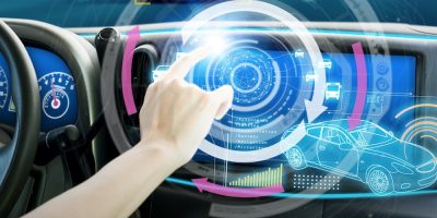
Geo Semiconductor chooses OmniVision image sensors

OmniVision Technologies’ OX03C10 automotive image sensor is combined with Geo Semiconductor’s automotive camera video processors (CVPs) in an automotive viewing camera.

The OmniVision’s OX03C10 is claimed to be the only automotive image sensor available that combines a large 3.0 micron pixel, high dynamic range (HDR) of 140dB for minimised motion artefacts, and the highest LED flicker mitigation (LFM) performance. The collaboration allows camera designers to process images captured by two image sensors with full HDR and LFM, using a single Geo CVP.

Intended for use in rear view cameras (RVCs), surround view systems (SVS) and e-mirrors, the image sensor takes advantage of the Geo GW5 CVP family’s ability to process 140dB HDR images with full LFM at 60 frames per second. The GW5 family’s advanced local tone mapping enables it to make optimal use of the OX03C10’s HDR and LFM image captures, adds OmniVision.

Using the GW5’s ability to process the captures from two image sensors simultaneously, with the HDR and LFM performance of OmniVision’s OX03C10 allows SVS camera designers to get the highest possible image quality without the added system bill of materials cost, complexity and power consumption of two CVPs, explains Geo.

The collaboration allows automotive designers to create the highest quality viewing cameras, across all lighting conditions, and in the presence of flickering LEDs from headlights, road signs and traffic signals, says the company.

This sensor’s integration of OmniVision’s HALE (HDR and LFM engine) combination algorithm provides the highest HDR and LFM performance simultaneously, claims Geo and the Deep Well dual conversion gain technology significantly reduces motion artefacts. Additionally, OmniVision’s split-pixel LFM technology with four captures provides the best performance over the entire automotive temperature range, claims the company. The OX03C10 is also the first viewing image sensor with HDR and LFM that can deliver 1920x1280p resolution at a frame rate of 60 frames per second, enabling faster camera view switching for drivers. The power consumption of the OX03C10 is 25 per cent lower than that of the nearest 2.5MP LFM image sensor, claims OmniVision and it has the industry’s smallest package size. As a result, cameras can continuously run at 60 frames per second and be placed in even the tightest spaces.

OmniVision’s PureCel Plus-S stacked architecture enables pixel performance advantages in the OX03C10 over non-stacked technology, in addition to a smaller die and lower power consumption. For example, 3D stacking allows OmniVision to boost pixel and dark current performance, resulting in a 20 per cent improvement in the signal-to-noise ratio (SNR) over the prior generation of its 2.5MP automotive viewing sensors.

The GW5 CVP family integrates an innovative HDR image signal processor (ISP) that supports the simultaneous 140dB HDR and industry’s highest LFM output of the OX03C10, providing great image detail in scenes with both bright and dark areas. Additionally, the GW5 includes Geo’s fifth-generation eWARP geometric processor to de-warp fish eye lenses exceeding a 180 degree wide field of view. The GW5 reduces system complexity and cost by requiring no external DDR memory and supporting dual sensor input that can process the captures from two OX03C10 sensors simultaneously, continues Geo.

OmniVision’s OX03C10 image sensor is available for sampling, and GEO’s GW5 CVP family is in mass production now. Both companies’ devices provide advanced ASIL functional safety and AEC-Q100 Grade 2 certification for automotive applications.

http://www.ovt.com

> Read More

SnapDragon and software stack drive ADAS and autonomous systems

Automotive software provider, Veoneer and Qualcomm have announced a collaboration to deliver scalable advanced driver assistance systems (ADAS), collaborative and autonomous driving (AD) solutions powered by Veoneer’s next-generation perception and driving policy software stack and Qualcomm’s Snapdragon Ride ADAS/AD scalable SoCs and accelerators. Qualcomm’s portfolio range from L1 to L4 systems designed to create an open platform for Tier-1 suppliers and vehicle manufacturers.

Veoneer’s software stacks are automotive grade solutions designed to meet the requirements of manufacturers, regulators and rating agencies globally. It has received top performance ratings and enabled automakers to achieve five star safety ratings for European New Car Assessment Program (Euro NCAP) in 2018 and 2020.

The companies plan to launch an automotive grade, functional safety compliant and optimised platform which will include a range of optimised NCAP features and up to hands-free driving on highways and slow-moving traffic with over the air updates.

The software stack will be developed in a dedicated organisation within Veoneer.

Designed to address the growing complexities associated with developing ADAS, including safety compliance, the integrated software and SoC platform targets the automotive ecosystem with advanced and power-efficient compute, connectivity and cloud service capabilities across all vehicle tiers with Veoneer’s fifth generation perception software and driving policy software and the Snapdragon Ride portfolio.

Qualcomm Technologies intends to make this integrated SoC and software stack platform available to global manufacturers and Tier 1 suppliers.

Veoneer will serve as a Tier 1 system integrator for the software and SoC platform and will continue to develop ADAS and collaborative driving products and systems.

The company will develop an open and programmable platform to offer more customisation. The companies expect the integrated platform to be available through automotive Tier 1 suppliers or directly to OEMs for 2024 vehicle production.

The Qualcomm Snapdragon Ride platform was introduced earlier this year. It is based on the Snapdragon family of automotive SoC and accelerator products, which are built on scalable and modular heterogenous, multi-core CPUs. This basis makes it suitable for planning and decision making, energy efficient AI and computer vision (CV) engines, graphics processor units (GPUs) for visualisation, image signal processors for camera sensors, and dedicated safety and security subsystems.

The integrated platform with Veoneer’s software stack will be built on the scalable Snapdragon Ride roadmap, offering industry leading scalability from L1 ADAS to L4 autonomous driving SoC and accelerator products.

http://www.veoneer.com

http://www.qualcomm.com

> Read More

Multi-channel RGB-LED driver support MeLiBu interface

Support for MeLiBu, the high speed communication interface differentiates the MLX81116 multi-channel RGB LED driver, says Melexis. The high speed communication IP enables automotive manufacturers to provide enhanced features in new models with smart interior lighting and to enable intelligent, automated lighting, continues the company.

MeLiBu is already being leveraged by leading manufacturers to enhance the safety features of their latest models. For example, animated lighting in the vehicle’s cabin can convey important driver assistance prompts and vehicle status information. An RGB LED lightbar communicates to the driver, through colour coding, colour changing, and blinking sequences.

Key engineering challenges for this systems include maintaining consistent colour across all the LEDs in the lightbar and ensuring they all change simultaneously. The MLX81116 addresses this through the high-speed communication interface IP, MeLiBu which controls individual LEDs separately in the lightbar to produce the lighting effects commanded by the vehicle. The intelligent RGB LED controller also provides real time compensation of any LED colour drift caused by environmental changes.

The MeLiBu communication interface uses the CAN-FD physical layer, which ensures robustness, reliability and high speed (up to 2Mbit), explains Melexis.  Support for dedicated optical parameters allows colour-mixing accuracy with a delta UV of one per cent to ensure no distinguishable differences between individual LEDs in the lightbar. In addition, intelligent high resolution for temperature-related colour drift helps maintain a consistent and non-distracting user experience under all operating conditions.

The MLX81116 driver IC has a wide dimming range that allows optimal brightness adjustment for daytime and night driving. It also meets automotive ISO 26262 functional safety requirements up to safety integrity level B (ASIL B) and features low EMI emission and high immunity, thanks to the use of the CAN-FD physical layer, which eases compliance with applicable EMC regulations, adds Melexis.

Melexis designs, develops and delivers mixed-signal semiconductor sensor and actuator components for integrating sensing, driving and communication into products and systems that improve safety, raise efficiency, support sustainability and enhance comfort.

Melexis has used its core experience in creating chips for vehicle electronics to expand its portfolio of sensors, driver ICs and wireless devices to also meet the needs of smart appliances, home automation, industrial and medical applications. Melexis sensing products include magnetic sensors, MEMS sensors (pressure, TPMS, infrared), sensor interface ICs, optoelectronic single point and linear array sensors and time of flight.

The company’s driver IC portfolio incorporates advanced DC and BLDC motor controllers, LED drivers and FET pre-driver ICs with the expertise to allow components to communicate whether wired or wireless.

Melexis is headquartered in Belgium.

http://www.melexis.com

> Read More

Two dual-output synchronous controllers are for automotive always-on systems

Claimed to draw the industry’s lowest 6microA quiescent current under light load conditions, the ISL78264 dual buck and ISL78263 boost-buck controllers are designed for automotive always-on systems.

The 42V dual synchronous controllers have low quiescent current and integrated 2A source/3A sink MOSFET drivers that provide primary power stage solutions for the Renesas R-Car H3 and R-Car M3 SoCs.

The ISL78264 dual sync buck controller and the ISL78263 dual sync boost and buck controller offer energy conserving low quiescent current over a single buck channel. Both controllers simplify power supply design by integrating FET drivers that can deliver industry leading 96 per cent peak efficiency and over 10A output current. They also integrate feedback resistors and an external supply blocking diode for applications requiring cranking support, and programmable spread spectrum for addressing EMI interference challenges, says Renesas Electronics. Built-in EMI mitigation, with a switching frequency up to 2.2 MHz, also reduces the cost and size of EMI filtering/shielding.

The ISL78264 dual sync buck controller manages the intermediate first stage DC/DC conversion, stepping down the 12V battery system to 5.0V and 3.3V to power the vehicle’s electronic control unit (ECU), in-vehicle infotainment (IVI) and digital cockpit systems with 50 to 200W power levels. The ISL78263 dual sync boost and buck controller provides DC/DC conversion to support power levels of 25 to 100W, while providing a pre-boost if the battery voltage (VBAT) dips to 2.1V during a crank transient or a start/stop event.

The ISL78264 and ISL78263’s always-on operation and industry’s lowest quiescent current gives power system designers the extra margin they need to stay within their 100 microA power budget, and can even manage tight budgets down to 50 microA, says Niall Lyne, vice president, Automotive Analog Power & Video business division at Renesas Electronics. “The controllers’. The ISL78264 and ISL78263 integrate strong MOSFET drivers that deliver higher efficiency and power compared to other automotive buck or boost VBAT controller solutions,” he adds.

The ISL78264 and ISL78263 also include extensive protection for over voltage (OV), under voltage (UV), over current, over temperature and a bootstrap supply under voltage detection and refresh circuit to protect the high side MOSFET.

Both controllers are AEC-Q100 Grade-1 qualified for ambient operation of -40 to +125 degrees C.

Mass production quantities of the ISL78264 dual synchronous buck controller and ISL78263 dual synchronous boost and buck controller are available now in 5.0 x 5.0mm, 32-lead wettable flank QFN packages.

http://www.renesas.com

> Read More

About Smart Cities

This news story is brought to you by smartcitieselectronics.com, the specialist site dedicated to delivering information about what’s new in the Smart City Electronics industry, with daily news updates, new products and industry news. To stay up-to-date, register to receive our weekly newsletters and keep yourself informed on the latest technology news and new products from around the globe. Simply click this link to register here: Smart Cities Registration