Microchip adds single-chip wireless platform designed for advanced connectivity

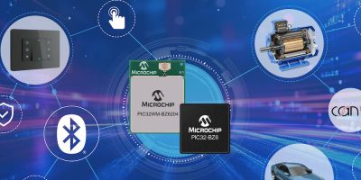
Microchip has released the highly integrated PIC32-BZ6 MCU that serves as a common, single-chip platform to reduce development cost, complexity and time-to-market for multi-protocol products featuring advanced connectivity and scalability.

RF design for smart devices has become increasingly complex, and wireless solutions typically require multiple chips to add new features or frequent redesigns to support evolving industry standards. The PIC32-BZ6 MCU replaces these multi-chip solutions and reduces the redesign burden with a single, highly integrated chip that removes the complexity of multi-protocol wired and wireless connectivity. The MCU also includes analog peripherals to simplify motor control development, along with touch and graphics capabilities for advanced user interfaces and enhanced memory to support complex applications, heavy workloads and Over the Air (OTA) firmware updates.

The PIC32-BZ6 MCU platform streamlines development of products in the smart home and for automotive connectivity, industrial automation and wireless motor control use cases. Key features include:

• High memory and scalable package choices to support demanding applications and OTA updates: The high-performance MCU includes 2 MB Flash memory and 512 KB RAM and is available in 132-pin ICs and modules with additional pin and package variants planned.
• Multi-protocol wireless networking: Qualified against Bluetooth Core Specification 6.0, the device also supports 802.15.4-based protocols such as Thread and Matter plus proprietary smart-home mesh networking protocols.
• Design flexibility that extends product options and scaling opportunities: Versatile and comprehensive selection of on-chip peripherals goes beyond wireless connectivity and OTA updates to support:
o Wired connectivity: Multiple interfaces include two CAN-FD ports for automotive and industrial communication, a 10/100 Mbps Ethernet MAC for high-speed wired connectivity and a USB 2.0 full-speed transceiver for seamless data transfer and PC integration.
o Touch and graphics: Incorporates peripherals that enable advanced user interfaces including Capacitive Voltage Divider (CVD)-based touch capabilities with up to 18 channels.
o Motor control: Simplifies system development through advanced analog peripherals such as 12-bit ADCs, 7-bit DAC, analog comparators, PWMs and QEI for precise motor position and speed control.
• Security by design to protect applications and IP: Includes immutable secure boot in ROM and an advanced on-board hardware-based security engine supporting AES, SHA, ECC and TRNG encryption.
• Reliability in harsh environments: The device is qualified to AEC-Q100 Grade 1 (125 °C) specifications for automotive and industrial environments.

Development Tools
Microchip simplifies development and product certification for the PIC32-BZ6 MCU by offering proven chip-down reference designs and wireless design check services, helping to minimise design risk. To further ease regulatory compliance, pre-certified modules are available in multiple regions worldwide. The PIC32-BZ6 MCU family is supported by the PIC32-BZ6 Curiosity Board that enables testing of all MCU I/Os, connectivity and peripheral features. Developers also benefit from a comprehensive development environment through Microchip’s MPLAB® Integrated Development Environment (IDE) and the Zephyr® Real Time Operating System (RTOS).

microchip.com

> Read More

ST’ half-bridge gate drivers ease design with GaN in low-voltage systems

ST’ STDRIVEG210 and STDRIVEG211 half-bridge gallium nitride (GaN) gate drivers are tailored for systems powered from industrial or telecom bus voltages, 72V battery systems, and 110V AC line-powered equipment. Rated for maximum rail voltage of 220V, the drivers integrate linear regulators to generate high-side and low-side 6 V gate signals and provide separate sink and source paths for optimum control.

The STDRIVEG210 is featured for power-conversion applications such as server and telecom supplies, battery chargers, adapters, solar micro-inverters and optimisers, LED lighting, and USB-C power sources. Suitable both for resonant and hard-switching topologies, its 300ns startup time permits to minimise the wake-up time especially during intermittent operation (burst mode).

The STDRIVEG211, equipped with overcurrent detection and smart shutdown, targets motor drives in power tools, e-bikes, pumps, and servos, as well as class-D audio amplifiers, in addition to power supplies.

Both devices simplify and minimise BOM by integrating the bootstrap diode to easily supply high-side driver. The separate gate-driving paths can sink 2.4A and source 1.0A to ensure fast switching transitions and easy dV/dt tuning. Protection features include interlocking to prevent cross conduction, while the high-side and low-side drivers have a short propagation delay with 10 ns matching time for low dead time operation. Under-voltage lockout (UVLO) prevents operating in low-efficiency or dangerous conditions and the STDRIVEG211, which is oriented towards motor-drive applications, has additional high-side UVLO protection.

The devices also have over-temperature protection and dV/dt immunity up to ±200V/ns, while input-voltage tolerance up to 20V helps simplify the controller interface circuitry. A standby pin facilitates power management and a separated power ground allows optimal Kelvin source gate driving or the use of a current shunt.

www.st.com 

> Read More

NXP’s new battery cell control IC family for new energy solutions

NXP Semiconductors has announced its new 18-channel Li-ion battery cell controller BMx7318/7518 IC family, designed for electric vehicle high-voltage battery management systems (HVBMS), industrial energy storage systems (ESS) and 48 V battery management systems. Based on NXP’s new advanced architecture with dedicated analog to digital converters (ADC) per channel, the family offers flexible and diverse part number selection with PIN-to-PIN compatibility between the device derivatives, providing customers with a cost-effective solution while improving the overall battery management system performance. The new IC family meets both automotive ASIL-C and industrial SIL-2 functional safety certifications.

As the global demand for scalable and cost-effective energy solutions grows, battery management systems need to strike a balance between accuracy, lifetime, reliability and flexibility. The BMx7318/7518 IC family’s new chip architecture reduces the need for external components by 50%,significantly lowering costs for OEMs and tier 1 suppliers by combining electromagnetic interference(EMI) immunity and one of the leading bulk current injection (BCI) robust designs. At the same time, the solution integrates analog front-end, battery junction box and gateway functions into a single chip(such as I-sense or SPI2TPL bridge). It supports semi-centralised BMS architectures and achieves system-level cost optimization while ensuring BMS stability.

The BMx7318/7518 adopts a new integrated circuit design to achieve complete independence of the cell sampling channel, avoid crosstalk, and improve filtering accuracy. The design supports flexible layout of up to 18 cells and has all-channel parallel balancing capability up to 150mA(supporting up 125°C ambient temperature), with a single channel reaching up to 300mA, significantly improving battery balancing efficiency. At the same time, the system has an ultra-low power mode (only 5µA) to meet the needs of long-term storage and overseas transportation, and a dedicated hardware alarm pin achieves rapid response to overcurrent events.

https://nxp.com

> Read More

Renesas announces new GaN FETs for high-density power conversion

Renesas has introduced three new high-voltage 650V GaN FETs for AI data centres and server power supply systems including the new 800V HVDC architecture, E-mobility charging, UPS battery backup devices, battery energy storage and solar inverters. Designed for multi-kilowatt-class applications, these 4th-generation plus (Gen IV Plus) devices combine high-efficiency GaN technology with a silicon-compatible gate drive input, significantly reducing switching power loss while retaining the operating simplicity of silicon FETs. Offered in TOLT, TO-247 and TOLL package options, the devices give engineers the flexibility to customise their thermal management and board design for specific power architectures.

The new TP65H030G4PRS, TP65H030G4PWS and TP65H030G4PQS devices leverage the SuperGaN platform, a field-proven depletion mode (d-mode) normally-off architecture pioneered by Transphorm, which was acquired by Renesas in June 2024. Based on low-loss d-mode technology, the devices offer efficiency over silicon, silicon carbide (SiC), and other GaN offerings. Moreover, they minimise power loss with lower gate charge, output capacitance, crossover loss, and dynamic resistance impact, with a higher 4V threshold voltage, which is not achievable with today’s enhancement mode (e-mode) GaN devices.

Built on a die that is 14 percent smaller than the previous Gen IV platform, the new Gen IV Plus products achieve a lower RDS(on) of 30 milliohms (mΩ), reducing on-resistance by 14 percent and delivering a 20 percent improvement in on-resistance output-capacitance-product figure of merit (FOM). The smaller die size reduces system costs and lowers output capacitance, which results in higher efficiency and power density.

Available in compact TOLT, TO-247 and TOLL packages, they provide one of the broadest packaging options to accommodate thermal performance and layout optimisation for power systems ranging from 1kW to 10kW, and even higher with paralleling. The new surface-mount packages include bottom side (TOLL) and top-side (TOLT) thermal conduction paths for cooler case temperatures, allowing easier device paralleling when higher conduction currents are needed. Further, the commonly used TO-247 package provides customers with higher thermal capability to achieve higher power.

Like previous d-mode GaN products, the new Renesas devices use an integrated low-voltage silicon MOSFET – a unique configuration that achieves seamless normally-off operation while fully capturing the low loss, high efficiency switching benefits of the high- voltage GaN. As they use silicon FETs for the input stage, the SuperGaN FETs are easy to drive with standard off-the-shelf gate drivers rather than specialised drivers that are normally required for e-mode GaN. This compatibility simplifies design and lowers the barrier to GaN adaptation for system developers.

GaN-based switching devices are quickly growing as key technologies for next-generation power semiconductors, fuelled by demand from electric vehicles (EVs), inverters, AI data centre servers, renewable energy, and industrial power conversion. Compared to SiC and silicon-based semiconductor switching devices, they provide superior efficiency, higher switching frequency and smaller footprints.

https://renesas.com/gan-fets.

> Read More

About Smart Cities

This news story is brought to you by smartcitieselectronics.com, the specialist site dedicated to delivering information about what’s new in the Smart City Electronics industry, with daily news updates, new products and industry news. To stay up-to-date, register to receive our weekly newsletters and keep yourself informed on the latest technology news and new products from around the globe. Simply click this link to register here: Smart Cities Registration