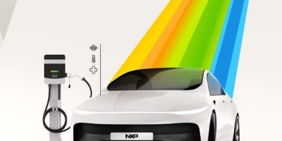
NXP’s new battery cell control IC family for new energy solutions

NXP Semiconductors has announced its new 18-channel Li-ion battery cell controller BMx7318/7518 IC family, designed for electric vehicle high-voltage battery management systems (HVBMS), industrial energy storage systems (ESS) and 48 V battery management systems. Based on NXP’s new advanced architecture with dedicated analog to digital converters (ADC) per channel, the family offers flexible and diverse part number selection with PIN-to-PIN compatibility between the device derivatives, providing customers with a cost-effective solution while improving the overall battery management system performance. The new IC family meets both automotive ASIL-C and industrial SIL-2 functional safety certifications.

As the global demand for scalable and cost-effective energy solutions grows, battery management systems need to strike a balance between accuracy, lifetime, reliability and flexibility. The BMx7318/7518 IC family’s new chip architecture reduces the need for external components by 50%,significantly lowering costs for OEMs and tier 1 suppliers by combining electromagnetic interference(EMI) immunity and one of the leading bulk current injection (BCI) robust designs. At the same time, the solution integrates analog front-end, battery junction box and gateway functions into a single chip(such as I-sense or SPI2TPL bridge). It supports semi-centralised BMS architectures and achieves system-level cost optimization while ensuring BMS stability.

The BMx7318/7518 adopts a new integrated circuit design to achieve complete independence of the cell sampling channel, avoid crosstalk, and improve filtering accuracy. The design supports flexible layout of up to 18 cells and has all-channel parallel balancing capability up to 150mA(supporting up 125°C ambient temperature), with a single channel reaching up to 300mA, significantly improving battery balancing efficiency. At the same time, the system has an ultra-low power mode (only 5µA) to meet the needs of long-term storage and overseas transportation, and a dedicated hardware alarm pin achieves rapid response to overcurrent events.

https://nxp.com

> Read More

Renesas announces new GaN FETs for high-density power conversion

Renesas has introduced three new high-voltage 650V GaN FETs for AI data centres and server power supply systems including the new 800V HVDC architecture, E-mobility charging, UPS battery backup devices, battery energy storage and solar inverters. Designed for multi-kilowatt-class applications, these 4th-generation plus (Gen IV Plus) devices combine high-efficiency GaN technology with a silicon-compatible gate drive input, significantly reducing switching power loss while retaining the operating simplicity of silicon FETs. Offered in TOLT, TO-247 and TOLL package options, the devices give engineers the flexibility to customise their thermal management and board design for specific power architectures.

The new TP65H030G4PRS, TP65H030G4PWS and TP65H030G4PQS devices leverage the SuperGaN platform, a field-proven depletion mode (d-mode) normally-off architecture pioneered by Transphorm, which was acquired by Renesas in June 2024. Based on low-loss d-mode technology, the devices offer efficiency over silicon, silicon carbide (SiC), and other GaN offerings. Moreover, they minimise power loss with lower gate charge, output capacitance, crossover loss, and dynamic resistance impact, with a higher 4V threshold voltage, which is not achievable with today’s enhancement mode (e-mode) GaN devices.

Built on a die that is 14 percent smaller than the previous Gen IV platform, the new Gen IV Plus products achieve a lower RDS(on) of 30 milliohms (mΩ), reducing on-resistance by 14 percent and delivering a 20 percent improvement in on-resistance output-capacitance-product figure of merit (FOM). The smaller die size reduces system costs and lowers output capacitance, which results in higher efficiency and power density.

Available in compact TOLT, TO-247 and TOLL packages, they provide one of the broadest packaging options to accommodate thermal performance and layout optimisation for power systems ranging from 1kW to 10kW, and even higher with paralleling. The new surface-mount packages include bottom side (TOLL) and top-side (TOLT) thermal conduction paths for cooler case temperatures, allowing easier device paralleling when higher conduction currents are needed. Further, the commonly used TO-247 package provides customers with higher thermal capability to achieve higher power.

Like previous d-mode GaN products, the new Renesas devices use an integrated low-voltage silicon MOSFET – a unique configuration that achieves seamless normally-off operation while fully capturing the low loss, high efficiency switching benefits of the high- voltage GaN. As they use silicon FETs for the input stage, the SuperGaN FETs are easy to drive with standard off-the-shelf gate drivers rather than specialised drivers that are normally required for e-mode GaN. This compatibility simplifies design and lowers the barrier to GaN adaptation for system developers.

GaN-based switching devices are quickly growing as key technologies for next-generation power semiconductors, fuelled by demand from electric vehicles (EVs), inverters, AI data centre servers, renewable energy, and industrial power conversion. Compared to SiC and silicon-based semiconductor switching devices, they provide superior efficiency, higher switching frequency and smaller footprints.

https://renesas.com/gan-fets.

> Read More

Microchip enhances their digital signal controller lineup

Evolving security and functional safety demands, coupled with the growing complexity of real-time embedded applications, are driving designers to seek innovative solutions that deliver greater accuracy, improved reliability and compliance with industry standards. To address these challenges, Microchip Technology has added the dsPIC33AK512MPS512 and dsPIC33AK512MC510 Digital Signal Controller (DSC) families to its dsPIC33A DSC product line. The devices enable the implementation of computation-intensive control algorithms for improved energy efficiency in motor control, AI server power supplies, energy storage systems and complex sensor signal processing with Machine Learning (ML)-based inferencing.

The dsPIC33AK512MPS family delivers precise, high-speed control through 78 ps high-resolution Pulse Width Modulations (PWMs) and low-latency 40 Msps ADCs, enabling fast and accurate control loops essential for optimising the performance of Silicon Carbide (SiC) and Gallium Nitride (GaN)-based DC-DC converters. Additionally, dsPIC33AK512MPS devices include advanced security features, an integrated touch controller and a high pin count of up to 128 pins. The dsPIC33AK512MC family is designed to offer low-latency, 40 Msps ADCs and 1.25 ns PWM resolution, providing a feature- and cost-optimised solution for multi-motor control and complex embedded applications.

The dsPIC33A DSC families, with up to 512 KB Flash and a rich peripheral set, integrate a double precision floating-point unit to accelerate mathematical computations and leverage a 32-bit architecture for seamless adoption of model-based design code. Their enhanced instruction set and Digital Signal Processing (DSP) capabilities, including single-cycle MAC operations and a 200 MHz core speed, make these devices highly efficient for low-latency, real-time control applications. Supported by MPLAB Machine Learning Development Suite, dsPIC33A devices streamline the ML workflow by automating data preparation, feature extraction, training, validation and firmware conversion of optimized models.

With a range of hardware safety features, dsPIC33AK512MPS/MC DSCs are compliant with functional safety standards and are developed in accordance with International Organisation for Standardisation (ISO) 26262 and International Electrotechnical Commission (IEC) 61508 processes, making them suitable for safety-critical automotive and industrial applications. To further enhance system-level security, the dsPIC33AK512MPS DSC family includes integrated crypto accelerators and a Flash security module, enabling immutable root of trust, secure boot, secure firmware upgrades and secure debug capabilities.

https://www.microchip.com

> Read More

Silanna launches industry’s smallest laser driver platform

Silanna Semiconductor has launched the FirePower series of laser driver ICs that reduce the size and increase the peak power of LiDAR applications.

FirePower Laser Driver ICs are the first to combine charging and firing on a single chip. This enables a significant reduction in size and losses as well as the removal of several components from the PCB to reduce the component count and BOM cost.

The integration also creates the ability to develop high-performance laser-based applications that deliver unmatched pulse power and precision. For example, using the IC enables a 400 W quad EEL (Edge-Emitting Laser) module to shrink from 400 mm2 to 80 mm2 (an 80% improvement), while enabling a 73% improvement in VIN-to-laser efficiency.

The first product to be launched in the FirePower family is the SL2001, a 14-pin 3.5 mm2 IC with a sub-2 ns FWHM laser pulse and dual drive for peak-power outputs of up to 1000 W.

The device has high charging efficiency and operates from a supply range of 3 V to 24 V to fire either EEL diodes or VCSELs (Vertical Cavity Surface Emitting Laser) with a pulse repetition frequency of over 10 MHz.

The SL2001 also has a differential Laser Fire output indication with a sub 0.1 ns Peak-to-Peak jitter. Built in laser output power sensing and control enables the SL2001 to meet eye-safety requirements. The device also uniquely implements programmability via an I2C interface and multi-time-programmable ROM, removing the need for an on-PCB MCU. The SL2001 can track and respond to both input voltage and resonant capacitor voltage.

The IC is targeted at LiDAR and other time-of-flight sensing systems used in industrial manufacturing, and automotive systems.

Product Marketing Director Ken Boyden said: “LiDAR and similar laser-based applications have traditionally relied on third party power supply regulators to meet the high voltage requirements of resonant pulsed laser systems. The FirePower family is the first to consolidate both highly efficient high voltage charging and high-power firing on a single chip. As the first product in the FirePower family, the SL2001 sets new benchmarks for performance and efficiency, while reducing component count and BOM cost.”

https://silannasemi.com

> Read More

About Smart Cities

This news story is brought to you by smartcitieselectronics.com, the specialist site dedicated to delivering information about what’s new in the Smart City Electronics industry, with daily news updates, new products and industry news. To stay up-to-date, register to receive our weekly newsletters and keep yourself informed on the latest technology news and new products from around the globe. Simply click this link to register here: Smart Cities Registration