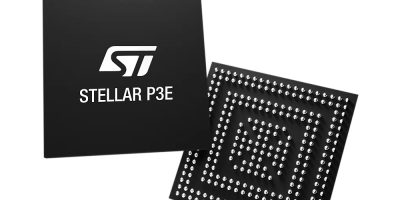
NXP’s new battery cell control IC family for new energy solutions

NXP Semiconductors has announced its new 18-channel Li-ion battery cell controller BMx7318/7518 IC family, designed for electric vehicle high-voltage battery management systems (HVBMS), industrial energy storage systems (ESS) and 48 V battery management systems. Based on NXP’s new advanced architecture with dedicated analog to digital converters (ADC) per channel, the family offers flexible and diverse part number selection with PIN-to-PIN compatibility between the device derivatives, providing customers with a cost-effective solution while improving the overall battery management system performance. The new IC family meets both automotive ASIL-C and industrial SIL-2 functional safety certifications.

As the global demand for scalable and cost-effective energy solutions grows, battery management systems need to strike a balance between accuracy, lifetime, reliability and flexibility. The BMx7318/7518 IC family’s new chip architecture reduces the need for external components by 50%,significantly lowering costs for OEMs and tier 1 suppliers by combining electromagnetic interference(EMI) immunity and one of the leading bulk current injection (BCI) robust designs. At the same time, the solution integrates analog front-end, battery junction box and gateway functions into a single chip(such as I-sense or SPI2TPL bridge). It supports semi-centralised BMS architectures and achieves system-level cost optimization while ensuring BMS stability.

The BMx7318/7518 adopts a new integrated circuit design to achieve complete independence of the cell sampling channel, avoid crosstalk, and improve filtering accuracy. The design supports flexible layout of up to 18 cells and has all-channel parallel balancing capability up to 150mA(supporting up 125°C ambient temperature), with a single channel reaching up to 300mA, significantly improving battery balancing efficiency. At the same time, the system has an ultra-low power mode (only 5µA) to meet the needs of long-term storage and overseas transportation, and a dedicated hardware alarm pin achieves rapid response to overcurrent events.

https://nxp.com

> Read More

Renesas announces new GaN FETs for high-density power conversion

Renesas has introduced three new high-voltage 650V GaN FETs for AI data centres and server power supply systems including the new 800V HVDC architecture, E-mobility charging, UPS battery backup devices, battery energy storage and solar inverters. Designed for multi-kilowatt-class applications, these 4th-generation plus (Gen IV Plus) devices combine high-efficiency GaN technology with a silicon-compatible gate drive input, significantly reducing switching power loss while retaining the operating simplicity of silicon FETs. Offered in TOLT, TO-247 and TOLL package options, the devices give engineers the flexibility to customise their thermal management and board design for specific power architectures.

The new TP65H030G4PRS, TP65H030G4PWS and TP65H030G4PQS devices leverage the SuperGaN platform, a field-proven depletion mode (d-mode) normally-off architecture pioneered by Transphorm, which was acquired by Renesas in June 2024. Based on low-loss d-mode technology, the devices offer efficiency over silicon, silicon carbide (SiC), and other GaN offerings. Moreover, they minimise power loss with lower gate charge, output capacitance, crossover loss, and dynamic resistance impact, with a higher 4V threshold voltage, which is not achievable with today’s enhancement mode (e-mode) GaN devices.

Built on a die that is 14 percent smaller than the previous Gen IV platform, the new Gen IV Plus products achieve a lower RDS(on) of 30 milliohms (mΩ), reducing on-resistance by 14 percent and delivering a 20 percent improvement in on-resistance output-capacitance-product figure of merit (FOM). The smaller die size reduces system costs and lowers output capacitance, which results in higher efficiency and power density.

Available in compact TOLT, TO-247 and TOLL packages, they provide one of the broadest packaging options to accommodate thermal performance and layout optimisation for power systems ranging from 1kW to 10kW, and even higher with paralleling. The new surface-mount packages include bottom side (TOLL) and top-side (TOLT) thermal conduction paths for cooler case temperatures, allowing easier device paralleling when higher conduction currents are needed. Further, the commonly used TO-247 package provides customers with higher thermal capability to achieve higher power.

Like previous d-mode GaN products, the new Renesas devices use an integrated low-voltage silicon MOSFET – a unique configuration that achieves seamless normally-off operation while fully capturing the low loss, high efficiency switching benefits of the high- voltage GaN. As they use silicon FETs for the input stage, the SuperGaN FETs are easy to drive with standard off-the-shelf gate drivers rather than specialised drivers that are normally required for e-mode GaN. This compatibility simplifies design and lowers the barrier to GaN adaptation for system developers.

GaN-based switching devices are quickly growing as key technologies for next-generation power semiconductors, fuelled by demand from electric vehicles (EVs), inverters, AI data centre servers, renewable energy, and industrial power conversion. Compared to SiC and silicon-based semiconductor switching devices, they provide superior efficiency, higher switching frequency and smaller footprints.

https://renesas.com/gan-fets.

> Read More

ROHM Introduces a new MOSFET for AI Servers

ROHM has released of a 100V power MOSFET, RY7P250BM, optimised for hot-swap circuits in 48V power systems used in AI servers and industrial power supplies requiring battery protection to the market.

As AI technology rapidly advances, data centres are facing unprecedented processing demands and server power consumption continues to increase annually. In particular, the growing use of generative AI and high-performance GPUs has created a need to simultaneously improve power efficiency while supporting higher currents. To address these challenges, the industry is shifting from 12V systems to more efficient 48V power architectures. Furthermore, in hot-swap circuits used to safely replace modules while servers remain powered on, MOSFETs are required that offer both wide SOA (Safe Operating Area) and low ON-resistance to protect against inrush current and overloads.

The RY7P250BM delivers these critical characteristics in a compact 8080-size package, helping to reduce power loss and cooling requirements in data centres while improving overall server reliability and energy efficiency. As the demand for 8080-size MOSFETs grows, this new product provides a drop-in replacement for existing designs. Notably, the RY7P250BM achieves wide SOA (VDS=48V, Pw=1ms/10ms) ideal for hot-swap operation. Power loss and heat generation are also minimised with an industry-leading low ON-resistance of 1.86mΩ (VGS=10V, ID=50A, Tj=25°C), approximately 18% lower than the typical 2.28mΩ of existing wide SOA 100V MOSFETs in the same size.

Wide SOA tolerance is essential in hot-swap circuits, especially those in AI servers that experience large inrush currents. The RY7P250BM meets this demand, achieving 16A at 10ms and 50A at 1ms, enabling support for high-load conditions conventional MOSFETs struggle to handle.

https://www.rohm.com

> Read More

ST’ off-line high-voltage converters boost space savings in consumer and lighting applications

STMicroelectronics’ new VIPer11B off-line high-voltage converters make tiny, efficient, and low-cost power supplies for applications up to 8W, including lighting, smart-home equipment, appliances, and smart meters.

ST’s VIPer11B converters cut the bill of materials through extensive feature integration to simplify circuit design and save external components. The 800V avalanche-rugged MOSFET requires only small snubbing components and a built-in senseFET provides almost lossless current sensing with no additional resistors. High-voltage startup circuitry is on-chip, requiring only an external capacitor for the Vcc supply, and the frequency-jittered oscillator minimises any external filtering needed to meet electromagnetic compatibility (EMC) regulations.

Also, being housed in a compact SSOP10 package, the converters deliver power where space is tight. This can be especially valuable in applications that are subject to rigidly defined form factors, such as LED-lighting drivers and smart bulbs. The converters also help meet stringent ecodesign regulations, with low standby current that cuts no-load power consumption to less than 10mW and pulse-skipping operation to boost light-load efficiency.

Flexibility is another strength, with a wide Vcc range that permits supplying the converter from a transformer auxiliary winding or from the output in a non-isolated topology. The VIPer11B can be used in non-isolated flyback, buck, and buck/boost topologies and isolated flyback with primary-side or secondary-side regulation.

Featuring output overload and overvoltage protection with automatic restart, Vcc clamping, thermal shutdown, and soft-start, VIPer11B converters help designers build strong and reliable power supplies. Two variants are available, letting designers select the VIPer113B with drain-current protection threshold of 370mA or the VIPer114B that has a current limit of 480mA.

https://www.st.com

> Read More

About Smart Cities

This news story is brought to you by smartcitieselectronics.com, the specialist site dedicated to delivering information about what’s new in the Smart City Electronics industry, with daily news updates, new products and industry news. To stay up-to-date, register to receive our weekly newsletters and keep yourself informed on the latest technology news and new products from around the globe. Simply click this link to register here: Smart Cities Registration