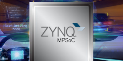
Mouser offers NXP’s i.MX 8M processors for A/V and smart home use

Semiconductor and components distributor, Mouser Electronics, now stocks the i.MX 8M family of applications processors from NXP Semiconductors. The i.MX 8M family is designed to enable embedded designers to meet the new standards of user interface, intelligence and connectivity set by consumer electronic devices. The processors can be used to increase video, graphic, and audio system requirements for smart home and smart IoT applications, such as streaming video devices, streaming audio devices, industrial tablets, medical and fitness, digital signage, and general-purpose human machine interface (HMI) solutions.

The NXP i.MX 8M processors integrate a general-purpose Arm Cortex-M4F core for real-time low-power processing, a GC7000Lite graphics processor, and either two (i.MX 8M Dual processors) or four (i.MX 8M Quad and QuadLite processors) Arm Cortex-A53 cores running at up to 1.5GHz.

The i.MX 8M quad and i.MX 8M dual processors have hardware acceleration for video playback up to 4K and video decoding in h.265, h.264 and VP9. Both processors support 32-bit audio samples with up a sampling rate to 768kHz. The i.MX 8M QuadLite processor allows for video playback with software decoders if needed, for graphics, processing performance, and high-speed interfaces.

 NXP’s i.MX 8M processors are supported by the i.MX 8MQuad evaluation kit, which provides several memory options, a 10/100/1000 Ethernet port, USB 3.0 connectors, and PCIe high-speed interfaces. The board includes connectors for HDMI 2.0, MIPI-DSI for local displays, two MIPI-CSIs for camera input, USB 3.0, Gigabit Ethernet, an audio interface expansion connector, and a 3.5 mm headphone jack.

Mouser strives to empower innovation among design engineers and buyers by delivering advanced technologies. It claims to stock the world’s widest selection of the latest semiconductors and electronic components for the newest design projects. Mouser Electronics’ website is continually updated and offers advanced search methods to help customers quickly locate inventory. Mouser.com also houses data sheets, supplier-specific reference designs, application notes, technical design information, and engineering tools.

http://www.mouser.com

> Read More

Power line communication (PLC) modem prepares for smart energy equipment

The PL360B PLC modem supports multiple standard and proprietary protocols used in smart grid infrastructure. According to Microchip, it enables manufacturers to respond to the utility companies’ need to improve the reliability and performance of smart meters and to address multiple markets, end-customer regulations and operational requirements. The single device can be adapted with firmware, reducing development costs and time to market.

The PL360B is designed to support PLC protocols in the frequency band up to 500kHz, such as ITU G.9903 (G3-PLC) and ITU G.9904 (Prime), as well as Cenelec, FCC and ARIB-compliant applications. The PL360B modem is supplied with reference designs for adding a PLC interface to any end-customer application requiring connectivity, including smart meters, lighting, home automation, building automation and remote control.

The PL360B modem offers up to a 25 per cent improvement in power consumption over previous generations, and has a Class D amplification scheme that optimises the modem transmission efficiency further.

The ATPL360 evaluation kit includes two evaluation boards to establish point-to-point communication. The kit includes PC tools designed to evaluate the performance of the PL360B, including a PHY tester for point-to-point test, PLC “sniffer” to capture PLC traffic in a deployed network and a PLC manager to manage the resulting network. G3-PLC and Prime-PLC communications firmware is provided free of charge.

A variety of reference designs is also available for a complete electricity meter with PLC, for a single PLC modem and for a master PLC device in charge of mastering the complete network of PLC nodes. All reference designs come with design files, bill of materials and schematics.

The PL360B and ATPL360 evaluation kit are available now.

This news story is brought to you by softei.com, the specialist site dedicated to delivering information about what’s new in the electronics industry, with daily news updates, new products and industry news.

To stay up-to-date, register to receive our weekly newsletters and keep informed of the latest technology news and new products from around the globe. Simply click this link to register here:  softei.com

Readers can also register to receive the monthly newsletter from our sister site, weartechdesign.com. This is the only website dedicated to developers of wearable electronic products. Simply click this link to register: weartechdesign.com

We have a Fitbit to give away on both Softei.com and Weartechdesign.com! Register today to enter the competition to win a Fitbit at softei.com or weartechdesign.com.

http://www.microchip.com/PL360B

> Read More

Signal switch ICs, clock generators and clock buffers chase 20Gbps protocols

Signal switches, clock generators and clock buffers for PCI Express (PCIe) 4.0 technology applications are now available from Diodes Incorporated

Addressing the expanding market for signal routing with different protocols in PCs, servers, embedded applications including artificial intelligence and fast data transfer generally, the PI3DBS16212 and PI3DBS16412 are 1-20Gbps 2-channel and 4-channel 2:1 differential multiplexers/demultiplexers with low loss, reflection, crosstalk and skew.

Offering greater flexibility of channels and routing, typical applications include switching high-speed serial signals employing the latest protocols, including: 20Gbps ThunderboltTM 3; 16Gbps PCIe 4.0 architecture; 10Gbps USB3.1 Gen2; 12Gbps Serial Attached SCSI 3 (SAS3); 8.1Gbps Display Port 4 (DP4); 12Gbps HDMI2.1, and 10Gbps Ethernet standards.

For the emerging PCIe 4.0 applications, the company says the PI3DBS16212 and PI3DBS16412 offer excellent signal integrity with an insertion loss of -1.3dB at 16Gbps. In this application, minimal skew between channels eases the timing budget between nodes, and power dissipation is low at typically 300-microA. The parts are fabricated with silicon on insulator (SOI) technology and have a small profile package at 2mm x 2mm for the 2:1 multiplexer.

Also driven by the adoption of the new PCIe 4.0 standard, the PI6CG18201, PI6CG18401, PI6CG18801, PI6CG15401 clock generators provide 1.8V 2/4/8 HCSL outputs and 1.5V 4 HCSL outputs, respectively, and use Diodes Incorporated’s proprietary phase-locked loop design to achieve the required tight jitter performance of less than 0.5ps.

The parts also provide the reference clock for SERDES chipsets supporting the PCIe 4.0 interface. Each output has its own enable with programmable slew rate and amplitude. On-chip termination resistors are incorporated saving up to 32 external resistors for the 8-channel version for space-constrained applications with the parts consuming about 85 per cent less power than traditional PCIe clocks. A spread-spectrum option is also available to reduce EMI in sensitive applications.

PI6CB18200, PI6CB18401, PI6CB18601, and PI6CB18801 are PCIe 4.0 2/4/6/8 HCSL output clock buffers fanned-out from a reference input. Like the clock generators, the slew rate and amplitude of each output is programmable and there are individual output enables for better power management. Additive jitter for the clock buffers is less than 0.05ps.

http://www.diodes.com

> Read More

Lattice claims low power FPGA will enable mass market AI in edge devices

Lattice Semiconductor believes its sensAI technology stack, combining modular hardware kits, neural network IP cores, software tools, reference designs and custom design services will open the door for rapid deployment of machine learning inference across IoT applications that require low power consumption.

The sensAI is optimised to provide low power operation (one mW to one W), small size, and production-priced (~one to $10) benefits of ASICs, with the flexibility of FPGAs, to support evolving algorithms, interfaces, and tailored performance, says Lattice.

These attributes are expected to accelerate deployment of AI into fast growth consumer and industrial IoT applications including mobile, smart home, smart city, smart factory, and smart car products.

The package size is 5.5 to 100mm2, while interface flexibility, with MIPI CSI-2, LVDS and GigE options, and the high-volume pricing offer a fast-track implementation of edge computing close to the source of data, says Lattice.

Deepak Boppana, senior director, product and segment marketing at Lattice Semiconductor said: “By delivering a full-featured machine learning inferencing technology stack combining flexible, ultra-low power FPGA hardware and software solutions, the Lattice sensAI stack accelerates integration of on-device sensor data processing and analytics in edge devices.” He goes on to say that the company’s expertise in FPGA technology are the basis for new edge computing solutions for edge connectivity, implementing flexible sensor interface bridging and data aggregation in high-volume IoT applications”, he continued, citing smart speakers, surveillance cameras, industrial robots and drones as potential applications.

“The edge is getting smarter with more computing capabilities being deployed for real-time processing of data from an expanding range of sensors, as seen in the consumer IoT space, and the emergence of artificial intelligence is only accelerating this trend,” said Michael Palma, research director at IDC.

With the adoption of machine learning technology, latency, privacy and network bandwidth limitations are pushing computing to the edge. IHS Markit expects 40 billion IoT devices at the edge between 2018 and 2025, and predicts that in the next five to 10 years, the convergence of IoT, AI-based edge computing and cloud analytics will disrupt “each and every industry vertical and domain, as well as to foster new business opportunities”. Semico Research predicts unit growth for edge devices with AI will increase by more than 110 per cent CAGR over the next five years.

Lattice’s sensAI stack includes modular hardware platforms, the ECP5 device-based video interface platform (VIP), including the Embedded Vision development kit, and iCE40 UltraPlus device-based Mobile Development Platform (MDP).

The IP core include the Convolutional Neural Network (CNN) accelerator and Binarised Neural Network (BNN) accelerator. Software tools are the neural network compiler tool for Caffe/TensorFlow to FPGA, Lattice Radiant design software and Lattice Diamond design software.

Face detection, key phrase detection, object counting, face tracking, and speed sign detection reference designs are also included, with design services from partners for market applications covering smart cities, smart homes and smart factories.

http://www.latticesemi.com

> Read More

About Smart Cities

This news story is brought to you by smartcitieselectronics.com, the specialist site dedicated to delivering information about what’s new in the Smart City Electronics industry, with daily news updates, new products and industry news. To stay up-to-date, register to receive our weekly newsletters and keep yourself informed on the latest technology news and new products from around the globe. Simply click this link to register here: Smart Cities Registration