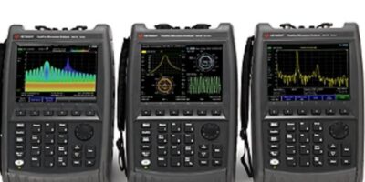
Farnell element14 offers Arm-based dev board to accelerate AI design

Availability of the Ultra96 development board has been announced by distributor, Farnell element14. The Arm-based Ultra96 development board was jointly created by Avnet, Xilinx, and 96Boards and is based on the Linaro 96Boards Consumer Edition specification. It features the Zynq UltraScale+ MPSoC with 2Gbit (512M x32) LPDDR4 RAM from Micron, 802.11b/g/n Wi-Fi and Bluetooth 4.2, one USB 3.0 Type Micro-B upstream port (for a device) and two USB 3.0 and one USB 2.0 Type A downstream ports (for hosts).

According to Farnell, it provides developers with a powerful environment to simplify machine learning. The 96Boards’ specifications are open and define a standard board layout for development platforms.

The Ultra96 is designed to offer a range of peripherals and has programmable logic acceleration engines for ‘complexity with simplicity’ according to the company. The Ultra96 allows software developers to accelerate the development process for applications that require intense processing and high performance in areas such as artificial intelligence (AI), machine learning, virtual reality, the IoT and industrial control.

Cliff Ortmeyer, global head of solutions development for Premier Farnell and Farnell element14 said: “The Ultra96 board combines Arm processing with programmable logic in a convenient, low-cost and expandable board which showcases a wide range of potential peripherals and acceleration engines that will help design engineers counter software bottlenecks.”

The Ultra96 boots from the industrial rated Delkin 16GB MicroSD card (supplied with the Ultra96 board), and is preloaded with Embedded Linux. Design engineers can connect to the Ultra96 through a web server using its integrated wireless access point capability, or use the pre-loaded Embedded Linux plus Enlightenment Desktop via integrated Mini DisplayPort video output. Multiple application examples and on-board development options are provided as examples.

The board includes four user-controllable LEDs. Design engineers can also interact with the board through the 96Boards-compatible low-speed and high-speed expansion connectors by adding peripheral accessories such as those included in Seeed Studio’s Grove Starter Kit for 96Boards.

The Ultra96 development board is available from Farnell element14 in EMEA, Newark element14 in North America and element14 in Asia Pacific.

http://www.premierfarnell.com

> Read More

Integrated open image signal processor adds to R-Car SoC applications

An integrated open image signal processor (ISP) from Renesas Electronics can be integrated on the company’s R-Car V3M and R-Car V3H SoCs to speed the development of automotive smart camera applications.

According to Renesas, integrating the ISP on the R-Car V3x SoCs and leveraging MM Solutions’ Automotive Camera Development Kit (AutoCDK), enables automotive Tier 1s to simplify the sensor calibration and tuning process for camera applications, including front camera and surround view to reduce the time to market.

The open ISP solution supports a range of development needs, from low-level-programming ISP capabilities via the open interface to the AutoCDK for users to jumpstart development using the MM Solutions’ tools.

Autonomous vehicles will be required to sense their environments, with smart cameras in front and surround view systems used to detect traffic signs, lanes, pedestrians, vehicles, and other obstacles in real time.

High performance computer vision requires highly reliable, highly configurable ISPs that support high dynamic ranges in challenging driving situations as well as low-noise performance and imagery perception close to that of a human eye’s level – or beyond, explains Renesas. Drivers will want to see a realistic visual representation of the surrounding of the car, where the ISP plays an important role for image adjustment.

In collaboration with MM Solutions, Renesas has developed an open ISP solution that helps users tune and control their sensors to support both human vision and machine vision. Integrating the ISP vision processing software onto the R-Car V3x SoCs provides a camera-neutral approach, offering camera manufacturers and Tier 1s the flexibility to work with ECUs and sensors of choice.

Jean-Francois Chouteau, vice president of the Automotive Solution Business Unit, Renesas Electronics, said: “Developing the software solution as part of the Renesas autonomy platform allows customers to take advantage of robust off-the-shelf middleware as well as privileged access to the image quality expertise of our partner MM Solutions.”

“Turnkey ISP solutions that support multiple platforms are essential to achieving excellent camera quality while meeting increasingly shorter time-to-market challenges for front camera, surround view, and other automotive camera applications,” added Ivan Poibrenski, managing director of MM Solutions.

“Achieving high dynamic range and LED flicker mitigation simultaneously is the key challenge for ADAS camera systems,” said Tsutomu Haruta, deputy senior general manager, Sony Semiconductor Solutions. “The combination of Renesas’ ISP solution and Sony’s image sensors enables our automotive customers to . . . realise a superior image quality.”

Mass production of the Renesas R-Car V3M and R-Car V3H SoCs is scheduled to begin Q2 2019 and Q3 2019, respectively. The AutoCDK from MM Solutions will be available in November 2018.

 Renesas will demonstrate the Open ISP using the Renesas R-Car V3M, MM Solutions’ AutoCDK, and Sony’s IMX390 image sensor in booth 6 at AutoSens 2018, September 17-20, 2018, Brussels, Belgium.

http://www.renesas.com

> Read More

H-bridge motor driver IC meets demand for low voltage, high current drive

For DC brushed motors and stepping motors, the TC78H651FNG is a dual H-bridge driver IC announced by Toshiba Electronics Europe.

The TC78H651FNG delivers performance at a low voltage (down to 1.8V) and high current (up to 1.6A) for equipment powered by dry-cell batteries. It is suitable for motor applications such as cameras and compact printers using 3.7V lithium-ion batteries, toys and home appliances, smart meters, and electronic locks using two 1.5V dry batteries, and devices using 5V USB power supplies.

IoT advances and wireless technologies are driving demand for applications that can be remotely controlled by smartphones and tablets, in turn stimulating demand for battery-powered motor control, argues Toshiba. Existing H-bridge driver ICs use bipolar technology which is stable at low voltage. However, the associated high levels of current consumption shorten battery life and increase losses leading to reduced motor torque.

The TC78H651FNG uses Toshiba’s DMOS process that is suitable for low voltage drives to reduce losses and current consumption, ICC is around 0.6mA in operating mode and virtually zero when in standby mode, claims Toshiba. This achieves a longer battery life and stable low voltage operation. The reduced on resistance of 0.22 Ohm for the high and low sides combined reduces IC losses and improves torque in the motor, even when powered at 1.8V.

The device is housed in a 5.0 x 6.4mm, 0.65mm pitch TSSOP16 package and supports forward, reverse and stop rotation modes. Inbuilt error detection functions for over-current protection, thermal shutdown and under-voltage lockout all contribute to ensuring a safe system.

http://toshiba.semicon-storage.com

> Read More

Akida architecture SoC places AI at the edge

Claiming to be the first company to bring a production spiking neural network architecture, the Akida Neuromorphic system-on-chip (NSoC), to market, BrainChip describes the NSoC as suitable for edge applications such as advanced driver assistance systems (ADAS), autonomous vehicles, drones, vision-guided robotics, surveillance and machine vision systems.   

The Akida NSoC is small, low cost and low power, adds the company. It is scalable, allowing users to network many Akida devices together to perform complex neural network training and inferencing for many markets including cybersecurity, financial technology and agricultural technology.

“The artificial intelligence acceleration chipset marketplace is expected to surpass US$60 billion by 2025,” said Aditya Kaul, research director at Tractica. He added: “Neuromorphic computing holds significant promise to accelerate AI, especially for low-power applications. As many of the technical hurdles are resolved, the industry will see the deployment of a new class of AI-optimised hardware over the next few years.”

The Akida NSoC uses a pure CMOS logic process, ensuring high yields and low cost. Spiking neural networks (SNNs) are inherently lower power than traditional convolutional neural networks (CNNs), as they replace the math-intensive convolutions and back-propagation training methods with biologically inspired neuron functions and feed-forward training methodologies.

BrainChip’s research has determined the optimal neuron model and training methods, bringing unprecedented efficiency and accuracy. Each Akida NSoC has effectively 1.2 million neurons and 10 billion synapses, representing 100 times better efficiency than neuromorphic test chips from Intel and IBM. Comparisons to leading CNN accelerator devices show similar performance gains of an order of magnitude better images/second/watt running industry standard benchmarks such as CIFAR-10 with comparable accuracy.

The Akida NSoC is designed for use as a standalone embedded accelerator or as a co-processor. It includes sensor interfaces for traditional pixel-based imaging, dynamic vision sensors (DVS), Lidar, audio, and analogue signals. It also has high-speed data interfaces such as PCI-Express, USB, and Ethernet. Embedded in the NSoC are data-to-spike converters designed to optimally convert popular data formats into spikes to train and be processed by the Akida Neuron fabric.

Spiking neural networks are inherently feed-forward dataflows, for both training and inference. Ingrained within the Akida neuron model are innovative training methodologies for supervised and unsupervised training. In the supervised mode, the initial layers of the network train themselves autonomously, while in the final fully-connected layers, labels can be applied, enabling these networks to function as classification networks. The Akida NSoC is designed to allow off-chip training in the Akida development environment, or on-chip training. An on-chip CPU is used to control the configuration of the Akida Neuron Fabric as well as off-chip communication of metadata.

The Akida development environment is available now for early access customers to begin the creation, training, and testing of spiking neural networks targeting the Akida NSoC. The Akida NSoC is expected to begin sampling in Q3 2019.

http://www.brainchip.com.

> Read More

About Smart Cities

This news story is brought to you by smartcitieselectronics.com, the specialist site dedicated to delivering information about what’s new in the Smart City Electronics industry, with daily news updates, new products and industry news. To stay up-to-date, register to receive our weekly newsletters and keep yourself informed on the latest technology news and new products from around the globe. Simply click this link to register here: Smart Cities Registration