Two software options for Anritsu’s Universal Wireless Test Set MT8870A measure RF characteristics of 3GPP-compliant LTE-V2X (PC5) devices.
The LTE-V2X Tx Measurement MX887068A and LTE-V2X Waveforms MV887068A software options are claimed to offer the industry’s fastest, fully automatic, non-signalling-based LTE-V2X TRx tests.
Customers can extend the MT8870A’s functionality by installing the software, with no need to invest in new equipment, says Anritsu.
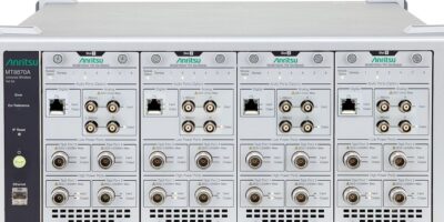
With four TRX measurement modules installed in the MT8870A, four devices under test (DUT) can be connected and measured simultaneously. Different wireless systems can also be measured in parallel, cutting measurement time and the space taken up by test equipment.
The software expands the capabilities of the Universal Wireless Test Set MT8870A, which is designed for mass-production test of multi-standard wireless systems. In addition to LTE-V2X and IEEE 802.11p(DSRC) for automotive solutions, the test set also supports the latest 5G sub-6GHz, LTE, NB-IoT, Cat-M, WLAN and Bluetooth standards.
Anritsu developed the MT8870A to increase the mass-production efficiency of V2X devices and chipsets and help to accelerate the launch of commercial C-V2X services.
Anritsu has provided communications test and measurement products for 120 years. Anritsu engages customers as true partners to help develop wireless, optical, microwave/RF, and digital solutions for R&D, manufacturing, installation, and maintenance applications, as well as multi-dimensional services for network monitoring and optimisation. Anritsu also provides precision microwave/RF components, optical devices, and high-speed electrical devices for communication products and systems. The company develops 5G, M2M, IoT, as well as emerging and legacy wireline and wireless communication markets.