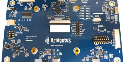
AN810-XNX edge AI computer leverages Jetson Xavier NX

For high speed networking, Aetina has introduced the AN810-XNX edge AI computer leveraging the capabilities of the Nvidia Jetson Xavier NX. This edge AI computer provides I/O options and expands Aetina’s range of edge AI systems for robotics, drone, unmanned aerial vehicles (UAV), industrial inspection, medical imaging, and deep learning.

The AN810-XNX combines the Nvidia Jetson Xavier NX and Aetina AN810 carrier board in a Nano-ITX form factor which measures 120 x 120 x 47.3 mm (with fan). It supports full M.2 slot with M-key, E-key, and B-key and the interface with PCIe/SATA/USB 3.2 Gen2/USB 2.0. AN810-XNX features prospective communication capabilities.

The AN810-XNX is integrated with the 4G/5G module for high speed wireless connection and data transfer. It is also equipped with an onboard SIM slot, building seamless global connectivity for edge devices. It also supports the Innodisk InnoAGE out-of-band management solid state device via M.2 to reduce the cost of manually repairing the edge device and primarily minimises the equipment’s downtime, making the remote control of the edge device more convenient.

For AI, the AN810-XNX supports the single 120-pin connector for MIPI CSI-2 interface and can handle intensive AI workloads using high resolution cameras for accurate image analysis. For back up support, Aetina offers board support package (BSP) and device tree blob (DTB) configuration updates for both standard and customised platforms in their service policy.

Nvidia Jetson supports cloud-native technologies across AI and various software development kits (SDKs). The Aetina AN810-XNX is Microsoft Azure-certified for the IoT, to accelerate development and to ensure operation with Microsoft Azure IoT services.

The AN810-XNX is available now.

Aetina was founded in Taiwan in 2012 as a provider of high-performance general purpose graphics processor units (GPGPU) and edge AI computing designs based on the Nvidia Jetson platform for embedded applications. The company provides industrial components, system integration and services focused on the industrial and AIoT market.

http://www.aetina.com

> Read More

Dual camera mezzanine aids fast prototyping in embedded vision systems 

To develop embedded vision applications with camera sensor modules at a low cost of entry, Avnet has introduced the 96Boards ON Semiconductor dual camera mezzanine development and prototyping platform for the AP1302 imaging processor coupled with dual imaging camera modules. The platform will enable design and system engineers to create cost-effective embedded vision applications using industry-standard technologies, says the distributor.

The two Imager Access System (IAS) camera modules on the mezzanine use the AR0144 monochrome digital image sensor from ON Semiconductor. The AR0144 is a 1Mpixel Mobile Industry Processor Interface (MIPI) sensor (1280 horizontal by 800 vertical resolution) and will run at 60 frames per second at full resolution. Its ability to capture clear images is critical for applications such as scanning, industrial inspection and drone navigation, explains the company.

By using the 96Boards standard, the card can enable low latency vision system prototyping by leveraging the capabilities of the Xilinx Ultra96-V2 platform.

“This prototyping platform is specially created for design engineers, system engineers and suppliers to focus on IoT vision, AI and computer imaging applications,” said Jim Beneke, vice president of products and emerging technologies, Avnet. “It simplifies the complex process of developing applications with imaging sensors. In addition, Avnet has matched this card with our Ultra96-V2 to provide a very high performance, cost effective AI vision platform.”

The platform uses MIPI and the camera serial interface (CSI2) standards which are specifications of the MIPI Alliance. The MIPI-CSI2 specification defines the interface between the image sensors, ISP and a host processor, and is widely used for high-speed communications output from image sensors in most embedded systems.

The API 1302 image co-processor from ON Semiconductor performs image processing functions within the platform, including turning, configuration and calibration of the sensors. These processing functions also help to reduce design efforts of developing an embedded camera system. The AP1302 interfaces the sensors and the host processor using MIPI-CSI2 lanes.

The Avnet-designed 96Boards ON Semiconductor dual camera mezzanine development and prototyping platform comes with two IAS sensor modules and an AP1302 imaging co-processor.

http://www.avnet.com

> Read More

Geo Semiconductor chooses OmniVision image sensors

OmniVision Technologies’ OX03C10 automotive image sensor is combined with Geo Semiconductor’s automotive camera video processors (CVPs) in an automotive viewing camera.

The OmniVision’s OX03C10 is claimed to be the only automotive image sensor available that combines a large 3.0 micron pixel, high dynamic range (HDR) of 140dB for minimised motion artefacts, and the highest LED flicker mitigation (LFM) performance. The collaboration allows camera designers to process images captured by two image sensors with full HDR and LFM, using a single Geo CVP.

Intended for use in rear view cameras (RVCs), surround view systems (SVS) and e-mirrors, the image sensor takes advantage of the Geo GW5 CVP family’s ability to process 140dB HDR images with full LFM at 60 frames per second. The GW5 family’s advanced local tone mapping enables it to make optimal use of the OX03C10’s HDR and LFM image captures, adds OmniVision.

Using the GW5’s ability to process the captures from two image sensors simultaneously, with the HDR and LFM performance of OmniVision’s OX03C10 allows SVS camera designers to get the highest possible image quality without the added system bill of materials cost, complexity and power consumption of two CVPs, explains Geo.

The collaboration allows automotive designers to create the highest quality viewing cameras, across all lighting conditions, and in the presence of flickering LEDs from headlights, road signs and traffic signals, says the company.

This sensor’s integration of OmniVision’s HALE (HDR and LFM engine) combination algorithm provides the highest HDR and LFM performance simultaneously, claims Geo and the Deep Well dual conversion gain technology significantly reduces motion artefacts. Additionally, OmniVision’s split-pixel LFM technology with four captures provides the best performance over the entire automotive temperature range, claims the company. The OX03C10 is also the first viewing image sensor with HDR and LFM that can deliver 1920x1280p resolution at a frame rate of 60 frames per second, enabling faster camera view switching for drivers. The power consumption of the OX03C10 is 25 per cent lower than that of the nearest 2.5MP LFM image sensor, claims OmniVision and it has the industry’s smallest package size. As a result, cameras can continuously run at 60 frames per second and be placed in even the tightest spaces.

OmniVision’s PureCel Plus-S stacked architecture enables pixel performance advantages in the OX03C10 over non-stacked technology, in addition to a smaller die and lower power consumption. For example, 3D stacking allows OmniVision to boost pixel and dark current performance, resulting in a 20 per cent improvement in the signal-to-noise ratio (SNR) over the prior generation of its 2.5MP automotive viewing sensors.

The GW5 CVP family integrates an innovative HDR image signal processor (ISP) that supports the simultaneous 140dB HDR and industry’s highest LFM output of the OX03C10, providing great image detail in scenes with both bright and dark areas. Additionally, the GW5 includes Geo’s fifth-generation eWARP geometric processor to de-warp fish eye lenses exceeding a 180 degree wide field of view. The GW5 reduces system complexity and cost by requiring no external DDR memory and supporting dual sensor input that can process the captures from two OX03C10 sensors simultaneously, continues Geo.

OmniVision’s OX03C10 image sensor is available for sampling, and GEO’s GW5 CVP family is in mass production now. Both companies’ devices provide advanced ASIL functional safety and AEC-Q100 Grade 2 certification for automotive applications.

http://www.ovt.com

> Read More

Rohde & Schwarz upgrades FSW analyser to 8.3GHz bandwidth

Extending the internal analysis bandwidth of the Rohde & Schwarz FSW signal and spectrum analyser, Rohde & Schwarz has introduced the FSW-B8001 option, which enables the signal and spectrum analyser to support an industry leading 8.3GHz internal analysis bandwidth. According to Rohde & Schwarz it offers unequalled dynamic range and sensitivity.

The R&S FSW covers an input frequency range of up to 90GHz, and is claimed to provide an unmatched dynamic range and sensitivity, precision and EVM performance. The analyser, equipped with the extended analysis bandwidth option and dedicated measurement applications, can be used to meet current and future test and measurement requirements for wideband signal analysis across different industries. The FSW can include pulse measurements of aerospace and defence radar systems, satellite payload testing and amplifier pre-distortion tests. The instrument also covers chirp analysis for automotive radar and research on the next generation of wireless communication.

Wideband acquisition makes it possible to analyse frequency hops in detail while examining different radar systems operating at different frequencies, when developing and verifying both radar systems and radar jammer systems.

In wireless communications, increased bandwidths use higher data throughput. For example, says Rohde & Schwarz, the IEEE 802.11ay standard for Wi-Fi supports channel bonding, which leads to signals with bandwidths greater than 8GHz. Suitable wideband T&M equipment is also needed for Gbit communications sub-THz bands, such as D-Band and G-Band, which have been viewed as potential frequency ranges for a future 6G wireless communication standard.

Satellite systems’ bandwidths are expected to increase to 3.0 or 5.0GHz at frequencies up to 90GHz, for example for high throughput satellites designed to support Tbit connectivity.

The R&S FSW-B8001 internal analysis bandwidth option is now available from

Rohde & Schwarz supplies customers in the fields of test and measurement, broadcast and media, aerospace, defence, security and networks and cybersecurity with communications, information and security products.

The company is headquartered in Munich, Germany, and has subsidiaries in more than 70 countries, with regional hubs in Asia and America.

https://www.rohde-schwarz.com

> Read More

About Smart Cities

This news story is brought to you by smartcitieselectronics.com, the specialist site dedicated to delivering information about what’s new in the Smart City Electronics industry, with daily news updates, new products and industry news. To stay up-to-date, register to receive our weekly newsletters and keep yourself informed on the latest technology news and new products from around the globe. Simply click this link to register here: Smart Cities Registration