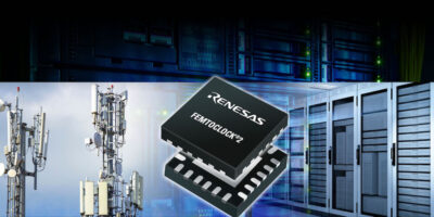
Wi-Fi 4 chip delivers next-generation WPA3 security

For cost-effective and secure IoT projects, the Infineon CYW43439 is a dedicated Wi-fi 4 chip which delivers the latest WPA3 security standard. The Wi-Fi/Bluetooth/Bluetooth Low Energy chip can be used for smart thermostats or smart lighting and other applications which need to comply with new security regulations, including the California Consumer Privacy Act which gives consumers the right to know the personal information a business collects, and the right for that information to be deleted.

Approximately half a billion new devices are expected to ship implementing Wi-Fi 4, the basic connectivity standard for the IoT, through 2025. Devices will be expected to support the latest features, such as WPA3.This security standard allows more robust authentication, increased cryptographic strength and more resilient mission-critical networks. Designers can use the Infineon CYW43439 to provide connectivity and implement the security standard in the product.

“For many IoT-connected products like smart thermostats and other consumer devices, their connectivity is both low bandwidth and low-duty cycles,” said Jeff Baer, senior product marketing director, IoT RF at Infineon. The CYW43439 allows customers to use the WPA3 security standard, and at the same time minimise connectivity cost by using Wi-Fi 4, he added.

With Wi-Fi 4, the CYW43439 enables robust, power-efficient performance, with worldwide certifications and certified interoperability. It can be used with RTOS, Linux, and Android platforms, and there is development support for software that includes advanced smart-coexistence for multi-user Wi-Fi and Bluetooth applications. This enables multiple connections simultaneously including Bluetooth Low Energy Mesh networking.

The devices reduce system power consumption by providing host SoC off-load processing for network management and audio applications reducing CPU loading. The optimised software for library-based functions allows connections to mobile devices or any cloud service at any time.

Infineon offers the CYW43439 with ModusToolbox software, describing it as an adaptable development systems for the IoT, with packaged solutions supporting popular ecosystems and cloud management tools.

The Infineon CYW43439 is available in volume quantities. Commercial modules are also available from industry-leading module partners.

http://www.infineon.com

> Read More

Intelligent IOLINK actuator reduces power by more than 50 per cent

Factory productivity is boosted by using the PD42-1-1243-IOLINK intelligent actuator, says Maxim Integrated, through monitoring 50 per cent more configuration and performance parameters. The Trinamic-branded intelligent actuator enables smart factories to quickly and remotely adjust an actuator’s electrical characteristics to minimise factory downtime and maximise throughput, says the company.

The PD42-1-1243-IOLINK combines a NEMA-17 stepper motor with controller and driver electronics and uses Maxim’s MAX22513 IO-Link transceiver to allow seamless configuring of all modes of Trinamic’s TMC2130-LA motor driver.

It is, says Maxim, the industry’s smallest, lowest-power NEMA-17 PANdrive actuator. It monitors 50 per cent more configuration and performance parameters to reduce commissioning times as well as to improve the quality of predictive maintenance data.

The TMC2130-LA motor driver and MAX22513 IO-Link transceiver chipset builds on the IO-Link’s two-way universal interface. The plug-and-play solution is 2.6x smaller and more than 50 per cent lower power compared to the competing solution, claims Maxim.

The MAX22513 IO-Link transceiver is supplied in a 4.2 x 2.1 WLP, which is three times smaller than the closest alternative currently available, Maxim says, making it the industry’s smallest ±1kV/500Ohm surge-protected, dual-driver IO-Link transceiver. It features high integration with a DC/DC regulator, protection diodes, auxiliary digital input, I²C or SPI control, integrated oscillator and selectable 3.3V or 5.0V LDO. It also enables four times lower power dissipation due to low 2.0 Ohm (typ) C/Q driver on-resistance compared to the nearest competing solution, according to Maxim.

The TMC2130-LA motor driver offers stall detection with no sensors necessary, to flag unwanted mechanical behaviour. It provides extremely smooth and precise motion with up to 256x microstepping compared to the 16x industry standard, resulting in accurate positioning and minimised resonance. Key integrated functions include a complete driver stage with low RDS(on) N-channel power MOSFETs configured as full H-bridges to drive the motor windings up to 1.2A RMS at 5.0 to 46V, an SPI for configuration and diagnostics, as well as a step-direction interface.

The PD42-1-1243-IOLINK increases productivity by adjusting more device parameters on-the-fly. It provides access to load values and noise reduction parameters using StealthChop technology to dynamically optimises the actuator throughout its operation.

TMC2130-LA’s CoolStep power savings feature, combined with MAX22513’s low RDS(on) N-channel power MOSFETS are claimed to provide best-in-class power savings compared to other NEMA-17 IO-Link drives on the market

Eliminating external limit switches to detect hard stop conditions results in a solution size of 82cm³, making it the smallest IO-Link intelligent actuator available today, says Maxim.

The PD42-1-1243-IOLINK is available at Trinamic’s authorised distributors.

Maxim Integrated is an engineer’s engineering company. It has a portfolio of high-performance semiconductors, combined with tools and support to deliver essential analogue solutions including efficient power, precision measurement, reliable connectivity and robust protection along with intelligent processing.

Designers in application areas such as automotive, communications, consumer, data centre, healthcare, industrial and the IoT make up the company’s customer base.

http://www.maximintegrated.com

> Read More

TrustAnchor provides simple path to automotive network security

Automotive OEMs and their module suppliers can use TrustAnchor to upgrade existing designs to meet security requirements, says Microchip. The cryptographic security IC supports in-vehicle network security solutions such as secure boot, firmware update and message authentication, including controller area network (CAN) MAC at bus speed, says Microchip.

The rise of in-vehicle network connections like Bluetooth and LTE/5G, means convenience but also more vulnerabilities in an automotive system. The TrustAnchor100 (TA100), CryptoAutomotive security IC helps OEMs and their module suppliers to simplify the upgrade of existing designs to meet security requirements for future generations.

To comply with new security specifications, automotive designers have to revise the vehicle’s electronic control units (ECUs) with secure hardware. Using single chip, dual core hardware security module (HSM) devices for this requires OEMs and module suppliers to rework application software to integrate the security element. This can introduce security holes, which can be overcome by third party security software but it will increase development costs.

The TA100 provides an alternative in-vehicle network architecture implementation for secure boot and message authentication. It has been approved by OEMs around the world as a solution for EVITA (e-safety vehicle intrusion protected applications) medium and full HSM requirements. Its feature set was designed following the review of OEM cybersecurity specifications. Microchip also offers security specification and request for quote (RFQ) review services to assist Tier 1s in developing educated responses.

According to Microchip, the TA100 removes the challenges associated with secure code development and provisioning by offering pre-programmed cryptographic internal application code provisioned with unique asymmetric key-pairs and associated x.509 certificates, thereby reducing risk, cost and time to market.

The device has high resistance to attack through intensive third-party vulnerability assessments, says Microchip and is AEC-Q100 Automotive Grade-1-qualified, FIPS 140-2 CMVP Security Level 2-rated and Physical Key Protection Level 3-certified. It has also achieved the highest possible vulnerability assessment rating of Joint Interpretation Library (JIL) High. The TA100 provides software components like AUTOSAR drivers, MCALs and Microchip’s CryptoAuthentication library for seamless integration into AUTOSAR, the industry standard OS, or customised software stacks for crypto functions.

The TA100 offers AUTOSAR-compliant MCAL drivers that can be integrated into an AUTOSAR software stack. A full AUTOSAR reference stack is available, enabling automotive vendors to deploy the latest crypto standards into automotive systems within standard automotive production environments, explains the company. MikroBUS-compatible socket boards are also available.

The TA100 is available in an eight- and 14-pin SOIC packages.

http://www.microchip.com

> Read More

Scalable AI SMARC SoM combo targets HMI and embedded vision

Comprising 10 Renesas ICs, the scalable system-on-module (SoM) Smart Mobility ARChitecture (SMARC) Winning Combination board accelerates development of artificial intelligence (AI) IoT face/object detection, image processing, and 4K video playback applications, says Renesas. The board can be used in surveillance cameras, inspection equipment, and industrial and building automation HMI and embedded vision systems.

The 10 ICs include microprocessor (MPU), power and analog ICs. The board is based on the SMARC 2.0 industry standard, which specifies an 82 x 80mm form factor. The SMARC SoM board offers designers a choice of three different scalable versions of the Renesas 64-bit RZ/G2 MPU. Options are an RZ/G2N dual core Arm Cortex-A57 MPU operating at 1.5 GHz for mid-range performance; the RZ/G2M MPU with dual-core Arm Cortex-A57 and quad-core Arm Cortex-A53 (1.2 GHz) for high performance; and the RZ/G2H MPU with quad-core Arm Cortex-A57 and quad-core Arm Cortex-A53 for what Renesas describes as ultra-high performance. All three MPUs (two cores up to eight cores) feature integrated 600MHz PowerVR 3D graphics and a 4K UHD H.265 and H.264 codecs to satisfy the needs of different computer processing requirements.

DK Singh, director, of the Systems and Solutions team at Renesas, said: “Our scalable solution’s extensive on-board interfaces, large memory and programmable clocks for different needs makes it an excellent turnkey solution for a wide range of applications. And its industry leading RZ/G2 MPUs with 3D graphics engine and 4K UHD and full HD video codec provides higher performance per dollar than competing 64-bit MPUs and GPUs.”

The SMARC SoM offers designers their choice of RZ/G2 MPU with up to 35.6k DMIPS performance, between 2.0 and 4Gbyte LPDDR4 RAM and 32Gbyte eMMC. Each RZ/G2 MPU is capable of running edge video analytics and AI frameworks. The MPUs feature an integrated AI software library, a set of interfaces, error checking and correction (ECC) protection on both internal and external memories, Linux OS, and a Verified Linux Package (VLP) which is tested and maintained by Renesas. There is also a Civil Infrastructure Platform (CIP) Super Long-Term Support (SLTS) kernel, and a Linux kernel bundled with a software development environment. The SMARC SoM board provides an optimised power and programmable timing tree. There is also support for dual-band Wi-Fi and Bluetooth Low Energy (BLE) for wireless communication, fast communication interfaces such as USB, SATA, LVDS, HDMI, CSI, I2S, PCIe, and Gigabit Ethernet, all accessible through the SMARC 2.0 connector.

The board includes the ISL1208 low-power real time clock for calendar-based applications powered by a small 400nA battery, or supercapacitor during a power failure and the P8330 power management IC (PMIC) for delivering power to multiple supply rails.

Also included are two clock sources, Renesas’ small form factor VersaClock 3S programmable clocks with integrated 32.768kHz DCO powered by a single coin cell battery during a power failure and a PCIe clock generated with the Renesas 9FGV0641. This supports six 100MHz differential clock outputs, with PCIe Gen 1 to 4 support

There is also the option for connection to two external cameras and LCD panel with capacitive touch.

The Scalable AI SMARC SoM Winning Combo Solution board was designed by Renesas and developed through a collaboration with RelySys Technologies. The board and design files are available now.

 http://www.renesas.com

> Read More

About Smart Cities

This news story is brought to you by smartcitieselectronics.com, the specialist site dedicated to delivering information about what’s new in the Smart City Electronics industry, with daily news updates, new products and industry news. To stay up-to-date, register to receive our weekly newsletters and keep yourself informed on the latest technology news and new products from around the globe. Simply click this link to register here: Smart Cities Registration