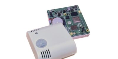
PICMG prepares the open COM-HPC specification for ratification

The latest open specification for high performance compute modules will be under review by members of the PICMG, a consortium for the development of open embedded computing specifications.

COM-HPC is the soon-to-be-released PICMG standard for high-performance computer-on-modules (COMs). COM-HPC defines five module sizes to deliver edge server performance for small, rugged data centres. The new specification will complement COM Express, which is expected to play a crucial role in the COM marketplace “for many years”.

PICMG developed the COM-HPC specification to address emerging requirements in the embedded and edge computing market. These have seen trends, including the substantial data growth and processing requirements of broadband and 5G as well as edge analytic including AI and situational awareness applications come to the fore. IoT devices, sensors, and actuators produce large amounts of data that require pre-processing at the edge for improved data processing efficiency and end to end security. Autonomous vehicles, smart factories, smart retail, medical robotics are among many applications that will benefit from increased edge server and edge client class processors processor modules or COMs available in standard modules that existing standards cannot meet.

The COM-HPC specification is based on two 400-pin, BGA mount, high-performance connectors and a system management interface. It is not limited to x86 processors and can be used with RISC processors, FPGAs and general purpose GPUs.

The COM-HPC client modules have up to 48 + 1 PCI Express Gen4/5 lanes, up to four USB4 ports and up to four video interfaces and one or two 25Gbit Ethernet interfaces.

Module sizes are 95 x 120mm (Size A), 120 x 120mm (Size B) and 160 x 120mm (Size C).

The COM-HPC server modules are characterised by up to 64 + 1 PCI Express Gen4/5 lanes, one or two USB4 ports, up to four graphic interfaces or are headless. There are up to eight 25Gbit Ethernet interfaces.

Module sizes are 160 x 160mm and 200 x 160mm (Sizes D and E respectively).

Founded in 1994, PICMG is a not-for-profit 501(c) consortium of companies and organisations that collaboratively develop open standards for high performance industrial, Industrial IoT, military and aerospace, telecommunications, test and measurement, medical, and general-purpose embedded computing applications. There are over 130 member companies that specialise in a wide range of technical disciplines, including mechanical and thermal design, single board computer design, high-speed signalling design and analysis, networking expertise, backplane, and packaging design, power management, high availability software and comprehensive system management.

Key standards families developed by PICMG include COM Express, CompactPCI, CompactPCI Serial, AdvancedTCA, MicroTCA, AdvancedMC, COM Express, SHB Express, MicroSAM, and HPM (Hardware Platform Management).

https://www.picmg.org

> Read More

Open and code-free software raises productivity for AI edge deployments

Claimed to be the industry’s first open and code-free software platform to span the complete edge AI operational workflow from idea to development, deployment and management, AI Studio is by Blaize. The company says it dramatically reduces edge AI application deployment complexity, time, and cost by breaking the barriers within existing application development and machine learning operations (MLOps) infrastructure. It eliminates the complexities of integrating disparate tools and workflows, and introduces multiple ease-of-use and intelligence features. According to Blaize, AI Studio reduces models moving to deployment to months from days.

AI studio introduces user interface, collaborative marketplaces, end-to-end application development and operational management. It can be deployed with the Blaize AI edge computing hardware for application development and MLOps.

The AI Studio code-free visual interface is intuitive, with speech commands such as “Hey Blaize” to summon a contextually intelligent assistant with an expert knowledge-driven recommendation system to guide users through the workflow.

Users can deploy models with one click to plug into any workflow across multiple open standards including ONNX, OpenVX, containers, Python, or GStreamer. According to Blaize, no other solution offers the same degree of open standard deployment support, as most are proprietary and lock in users with limited options. Support for these open standards allows AI Studio to deploy to any hardware that fully supports the standards.

Marketplaces support allows users to discover models, data and complete applications from public or private networks and to collaborate continuously to build and deploy AI applications.

AI Studio supports open public models, data marketplaces and repositories, and provides connectivity and infrastructure to host private marketplaces. Users can continually scale proven AI edge models and vertical AI solutions to effectively reuse across enterprises, choosing from hundreds of models with drag and drop ease to speed application development

The AI Studio model development workflow allows users to easily train and optimise models for specific datasets and use cases, and deploy quickly into multiple formats and packages. Its Transfer Learning feature quickly retrains imported models for the user’s data and use case. Another feature is the edge-aware optimisation tool, NetDeploy, which automatically optimises the models to the user’s specific accuracy and performance needs. Users can build and customise complete application flows other than neural networks, such as image signal processing, tracking or sensor fusion functions.

AI Studio helps users deploy, manage, monitor and continuously improve their edge AI applications. It is built on a cloud-native infrastructure based on microservices, containers and Kubernetes, for scalable and reliable production, says Blaize.

Application areas are smart retail, smart city and industry 4.0 projects. AI Studio is available now to qualified early adopter customers, with general availability in Q1 2021. The AI Studio product offering includes licenses for individual seats, enterprise, and on-premise subscriptions, with product features and services suited to the needs of each license type.

http://www.blaize.com

> Read More

800G test from Keysight Technologies validates next-gen data centres

Keysight Technologies has released 800G test solutions for validating electrical and optical interfaces to speed development of next-generation data centre technologies, including what is believed to be the first 100Gbits per second transmitter and receiver pre-conformance test.

Service providers and data centre operators are seeking 800G technology to meet a growing demand in network capacity at the desired cost and power consumption targets. This is primarily driven by data-hungry applications such as video conferencing, streaming and digital entertainment, which are delivered via wireless technologies such as 4G, 5G and Wi-Fi.

Electrical and optical analysis enables an 800G ecosystem, consisting of optical components, chipset, switch and semiconductor IC vendors, as well as system integrators, to speed design, development, test and validation across the entire design cycle.

Dr. Joachim Peerlings, vice president of network and data centre solutions at Keysight Technologies, said: “Access to a portfolio of 800G test solutions across physical and protocol layers, from simulation to design, validation, conformance and manufacturing, enables our customers to verify interoperability and simplify testing across the workflow using common, uniform interfaces and software automation.”

Keysight Technologies’ 800G test solutions include a 100Gbits per second electrical conformance test. It is believed to be first pre-conformance test solution for validating both transmitter and receiver electrical signalling input interfaces according to the 100Gb/s standard currently under development by the Institute of Electrical and Electronics Engineers (IEEE) and the Optical Internetworking Forum (OIF).

It also includes Keysight’s Infiniium UXR-Series real-time oscilloscope or digital communication analyser (DCA), 64Gbaud high performance bit error rate tester (BERT) and pre-conformance test cases for simplified 100, 200, 400 and 800Gbits per second electrical input interface testing, resulting in accurate and repeatable test results.

There is pre-silicon design verification, combining Keysight’s IxVerify software, which generates network traffic, with the Synopsys ZeBu Server 4 emulation system to accelerate pre-silicon design verification of SoCs and 800G Ethernet designs.

This delivers consistent test methodologies, configurations and scripts to accelerate testing from pre-silicon to post-silicon device validation.

A 200Gbits per second option is designed for 800G research and pathfinding. It combines an arbitrary waveform generator (AWG) and an Infiniium UXR-Series real-time oscilloscope to characterise the digital interface including error detection up to 224Gbits per second.

To extend testing into the optical domain, developers can use Keysight’s 60GHz optical-to-electrical (O/E) converter.

The physical layer test system (PLTS) establishes signal integrity measurements and performs data post processing of high speed interconnects, such as cables, backplanes, PCBs and connectors.

It supports de-embedding techniques on a common platform, enabling users to optimise performance margins in 800G channel designs.

According to Keysight, the components are designed to allow users to fully explore design margins, while addressing design and conformance validation challenges in an 800G transceiver market, which is expected to reach $2.5 billion by 2029 according analyst, CIR.

http://www.keysight.com

> Read More

MEMS accelerometer reduces space needed in challenging environments

A miniature, one-axis, closed loop MEMS accelerometer from TDK has a 24-bit digital SPI and SMD package. The Tronic AXO315 is claimed to match the performance of quartz sensors and outperforms commercial MEMS sensors.

The force-rebalance accelerometer delivers a one year composite bias repeatability of 1mg and composite scale factor repeatability of 600 ppm under severe temperature and vibration conditions common in industrial, land, railway, naval and construction applications. TDK says these characteristics enable significant reduction in size, weight and cost of materials for industrial motion control units, inertial measurement units (IMU) and inertial navigation systems (INS).

The AXO315 is a ±14g range, in-plane linear accelerometer. It has been designed and developed to provide high precision and reliability in challenging environments. It achieves a 1 mg composite bias repeatability over one year at temperatures ranging from -55 to +105 degrees C, and 4 g vibrations with vibration rejection. Performance is augmented by Allan variance characteristics and bias instability of 4 micro g, a velocity random walk of 0.006 m/s/√h, and very low noise of 15 micro g/√Hz, for high resolution and low error.

The AXO315’s performance is equivalent to the incumbent analogue quartz accelerometers and mechanical inclinometers, but at a fraction of their size, weight, and price. They also remain free from dual-use export control according to Annex 1 of Council Regulation (EC) No 428/2009. AXO315 exhibits higher performance levels than any current commercially available MEMS sensors components, says TDK. It delivers an 80 per cent gain in temperature stability compared to Tronics’ AXO215 accelerometer. The AXO315 accelerometer comes in a lightweight 1.4 g hermetic SMD J-lead ceramic package (measuring 12 x 12 x 5.0mm), enabling low-cost assembly and reliability on PCB, even in fast-changing temperature conditions.

The AXO315 can be used for applications requiring high accuracy and stability in demanding environments, such as servo inclinometers and dynamic inclinometers in industrial motion control units, IMUs and INS for GNSS-aided positioning, and navigation of manned and unmanned ground vehicles and trains.

The AXO315 accelerometers are manufactured, tested and calibrated at Tronics Microsystems’ facility in Grenoble, France.

Pre-production and customer sampling have begun. Evaluation of the sensors can also be made through an Arduino-based evaluation kit that is specifically designed to provide developers with improved testing functionalities such as output reading and recording, recalibration and digital self-tests. Full production of the sensors and availability through its network of distributors are scheduled for summer 2021.

Tronics Microsystems SA is a division of TDK’s Temperature & Pressure Sensors Business Group that manufactures custom MEMS products and standard inertial sensors. It provides custom and standard products especially to the industrial, aeronautics, security, and medical markets. Founded in 1997, Tronics is located in Crolles, near Grenoble (France) and in Dallas, Texas (United States).

http://www.tdk.com

> Read More

About Smart Cities

This news story is brought to you by smartcitieselectronics.com, the specialist site dedicated to delivering information about what’s new in the Smart City Electronics industry, with daily news updates, new products and industry news. To stay up-to-date, register to receive our weekly newsletters and keep yourself informed on the latest technology news and new products from around the globe. Simply click this link to register here: Smart Cities Registration