Swedish company, Epishine, which manufactures printed organic solar cells and development kits, has signed a franchise agreement with Farnell, an Avnet company. Farnell says it is the first high service distributor to stock products from the company.
The printed organic solar cells are optimised for harvesting energy from indoor, low energy lighting enabling organic solar power to be used everywhere. Design engineers can use this technology with Epishine’s light energy harvesting evaluation kit.
Epishine’s organic solar cells are small, thin, flexible, and printed on recyclable plastic. The cells can be integrated into any low power electronic equipment where they convert ambient indoor light into electricity. The organic solar cells can replace batteries in new-build wireless sensors and similar devices, reducing the environmental impact of battery waste and saving battery replacement costs, said Farnell.
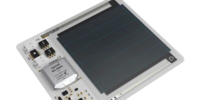
The EK01LEH3_6 light energy harvesting evaluation kit demonstrates how Epishine’s light energy harvesting (LEH) modules can power indoor wireless low-power devices that are usually powered by batteries. It combines a six-cell 50 x 50mm LEH module with a supercapacitor which acts as an energy buffer and intelligent charging management system to support various output voltages and energy storage solutions. An external primary battery can be used as a back up. The evaluation kit can deliver sufficient output current to power most low-power wireless devices such as Bluetooth Low Energy, Zigbee and LoRa. The programmable evaluation kit are optimised for indoor use (-20 to +40 degrees C / 0 to 85 per cent RH) with illumination intensities of 20 to 1,000 lux
It also includes a supercapacitor for energy storage which can be reconfigured to charge rechargeable battery.
Epishine’s organic solar cells will be added to Farnell’s line card later this year.
Founded in 2016, Epishine is a Swedish technology company which manufactures flexible organic light modules and a development kit to help engineers design new products that are normally powered by batteries. The light modules can be used to partly or completely power wireless sensors and similar devices required in our increasingly connected world.
Epishine’s manufacturing process is claimed to provide industry-leading efficiency in low light conditions. The company was founded in 2016 and has 25 employees with its headquarters, lab and manufacturing located in Linköping, Sweden.
Farnell offers a range of products in its comprehensive semiconductor portfolio to support design engineers. Customers also have free access to online resources, datasheets, application notes, videos, webinars and 24/5 technical support.